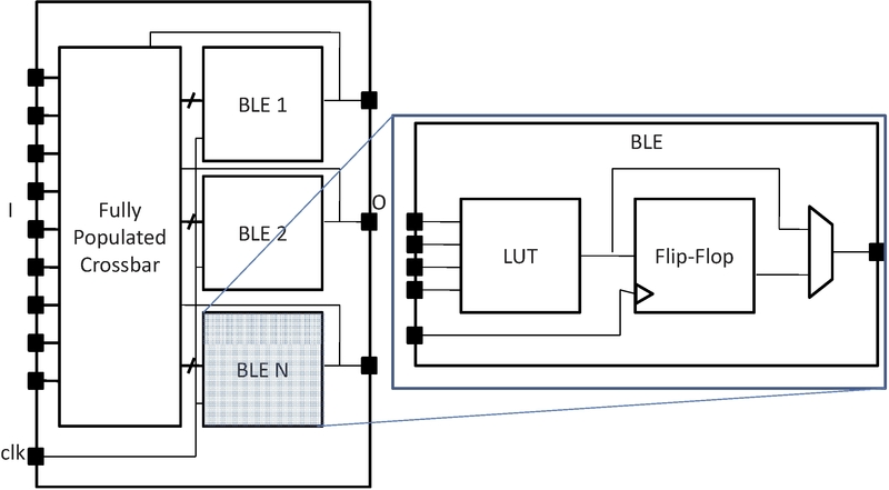
Figure 1: Model of a classical FPGA soft logic cluster
The following is an example on how to use the VPR 6.0 architecture description langauge to describe a classical academic soft logic block. First we provide a step-by-step explanation on how to construct the logic block. Afterwards, we present the complete code for the logic block.
Figure 1: Model of a classical FPGA soft logic cluster
Figure 1 shows an example of a classical soft logic block found in academic FPGA literature. This block consists of N Basic Logic Elements (BLEs). The BLE inputs can come from either the inputs to the logic block or from other BLEs within the logic block via a full crossbar. The logic block in this figure has I general inputs, one clock input, and N outputs (where each output corresponds to a BLE). A BLE can implement three configurations: a K-input look-up table (K-LUT), a flip-flop, or a K-LUT followed by a flip-flop. The structure of a classical soft logic block results in a property known as logical equivalence for certain groupings of input/output pins. Logically equivalent pins means that connections to those pins can be swapped without changing functionality. For example, the input to AND gates are logically equivalent while the inputs to a 4-bit adders are not logically equivalent. In the case of a classical soft logic block, all input pins are logically equivalent (due to the fully populated crossbar) and all output pins are logically equivalent (because one can swap any two BLEs without changing functionality). Logical equivalence is important because it enables the CAD tools to make optimizations especially during routing. We describe a classical soft logic block with N = 10, I = 22, and K = 4 below.
First, a complex block pb_type called CLB is declared with appropriate input, output and clock ports. Logical equivalence is labelled at ports where it applies:
<pb_type name="clb">
  <input name="I" num_pins="22" equivalent="true"/>
  <output name="O" num_pins="10" equivalent="true"/>
  <clock name="clk" equivalent="false"/>
A CLB contains 10 BLEs. Each BLE has 4 inputs, one output, and one clock. A BLE block and its inputs and outputs are specified as follows:
  <pb_type name="ble" num_pb="10">
    <input name="in" num_pins="4"/>
    <output name="out" num_pins="1"/>
    <clock name="clk"/>
A BLE consists of one LUT and one flip-flop (FF). Both of these are primitives. Recall that primitive physical blocks must have a blif_model attribute that matches with the model name in the BLIF input netlist. For the LUT, the model is ``.names'' in BLIF. For the FF, the model is ``.latch'' in BLIF. The class construct denotes that these are special (common) primitives. The primitives contained in the BLE are specified as:
    <pb_type name="lut_4" blif_model=".names" num_pb="1" class="lut">
      <input name="in" num_pins="4" port_class="lut_in"/>
      <output name="out" num_pins="1" port_class="lut_out"/>
    </pb_type>
    <pb_type name="ff" blif_model=".latch" num_pb="1" class="flipflop">
      <input name="D" num_pins="1" port_class="D"/>
      <output name="Q" num_pins="1" port_class="Q"/>
      <clock name="clk" port_class="clock"/>
    </pb_type>
Figure 2 shows the ports of the BLE with the
input and output pin sets. The inputs to the LUT and flip-flop are
direct connections. The multiplexer allows the BLE output
to be either the LUT output or the flip-flop output.
The code to specify the interconnect is:
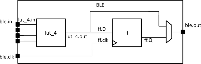
Figure 2: Internal names of BLE.
    <interconnect>
      <direct input="lut_4.out" output="ff.D"/>
      <direct input="ble.in" output="lut_4.in"/>
      <mux input="ff.Q lut_4.out" output="ble.out"/>
      <direct input="ble.clk" output="ff.clk"/>
    </interconnect>
  </pb_type>
The CLB interconnect is then modeled (see
Figure 1). The inputs to the 10 BLEs
(ble[9:0].in) can be connected to any of the CLB inputs
(clb.I) or any of the BLE outputs (ble[9:0].out) by
using a full crossbar. The clock of the CLB is wired to multiple BLE
clocks, and is modeled as a full crossbar. The outputs of the BLEs
have direct wired connections to the outputs of the CLB and this is
specified using one direct tag. The CLB interconnect
specification is:
  <interconnect>
    <complete input="{clb.I ble[9:0].out}" output="ble[9:0].in"/>
    <complete input="clb.clk" output="ble[9:0].clk"/>
    <direct input="ble[9:0].out" output="clb.O"/>
  </interconnect>
Finally, we model the connectivity between the CLB and the general FPGA fabric (recall that a CLB communicates with other CLBs and I/Os using general-purpose interconnect). The ratio of tracks that a particular input/output pin of the
CLB connects to is defined by fc_in/fc_out. In this example, a fc_in of 0.15 means that each input pin connects to 15% of the available routing tracks in the external-to-CLB routing channel adjacent to that pin. The pinlocations tag is used to associate pins on the CLB with which side of the logic block pins reside on
where the pattern spread corresponds to evenly spreading out the pins on all sides of the CLB in a round-robin fashion. In this example, the CLB has a total of 33 pins (22 input pins, 10 output pins, 1 clock pin) so 8 pins are assigned to all sides of the CLB except one side which gets assigned 9 pins. The columns
occupied by complex blocks of type CLB is defined by gridlocations where fill means that all columns should be type CLB unless that column
is taken up by a block with higher priority (where a larger number means a higher priority).
  <!-- Describe complex block relation with FPGA -->

  <fc_in type="frac">0.150000</fc_in>
  <fc_out type="frac">0.125000</fc_out>

  <pinlocations pattern="spread"/>
  <gridlocations>
    <loc type="fill" priority="1"/>
  </gridlocations>
</pb_type>
<!--
Example of a classical FPGA soft logic block with
N = 10, K = 4, I = 22, O = 10
BLEs consisting of a single LUT followed by a flip-flop that can be bypassed
-->

<pb_type name="clb">
  <input name="I" num_pins="22" equivalent="true"/>
  <output name="O" num_pins="10" equivalent="true"/>
  <clock name="clk" equivalent="false"/>

  <pb_type name="ble" num_pb="10">
    <input name="in" num_pins="4"/>
    <output name="out" num_pins="1"/>
    <clock name="clk"/>

    <pb_type name="lut_4" blif_model=".names" num_pb="1" class="lut">
      <input name="in" num_pins="4" port_class="lut_in"/>
      <output name="out" num_pins="1" port_class="lut_out"/>
    </pb_type>
    <pb_type name="ff" blif_model=".latch" num_pb="1" class="flipflop">
      <input name="D" num_pins="1" port_class="D"/>
      <output name="Q" num_pins="1" port_class="Q"/>
      <clock name="clk" port_class="clock"/>
    </pb_type>

    <interconnect>
      <direct input="lut_4.out" output="ff.D"/>
      <direct input="ble.in" output="lut_4.in"/>
      <mux input="ff.Q lut_4.out" output="ble.out"/>
      <direct input="ble.clk" output="ff.clk"/>
    </interconnect>
  </pb_type>

  <interconnect>
    <complete input="{clb.I ble[9:0].out}" output="ble[9:0].in"/>
    <complete input="clb.clk" output="ble[9:0].clk"/>
    <direct input="ble[9:0].out" output="clb.O"/>
  </interconnect>

  <!-- Describe complex block relation with FPGA -->

  <fc_in type="frac">0.150000</fc_in>
  <fc_out type="frac">0.125000</fc_out>

  <pinlocations pattern="spread"/>
  <gridlocations>
    <loc type="fill" priority="1"/>
  </gridlocations>
</pb_type>