1.0
Purpose
The purpose of
this lab is to learn about the basic operation of sequential logic (circuits
with memory), by building them up from basic gates. You will also build a shift
register from flip flops, and learn how to invoke flip-flops from the Verilog
language. As a side-effect of building bigger things from smaller things, we
illustrate the concept and use of hierarchy in design.
2.0
Background
In class we have
covered the basic circuit for RS latches, D latches, clocked D latches and
master-slave edge triggered D flip-flops, so you should review your notes on
these.
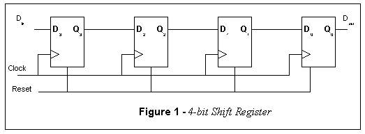
A shift register is typically used to
send and receive data, one bit at a time, under the control of a clock signal.
Figure 1 below illustrates a 4-bit shift register built out of
positive-edge triggered D-type flip flops. On each positive clock edge, the
value of the signal Di is copied onto the value of
Qi. Thus it takes four clock cycles for the
original value of Din to appear as Dout. The entire contents of the shift register can be
initialized by resetting each flip-flop with a reset signal.
3.0 Preparation
Design and
simulate (using timing simulation) the following circuits, using the graphic
editor of Quartus (DO NOT USE Verilog, except for
part 5). You should design all of these circuits with gates from the basic
logic primitives library. Make a separate directory for each of the circuits
you design. Parts 1, 2, and 3 concern the basic operation of circuits that have
memory, and so we have you design these from basic gates. Part 3 also
demonstrates the use of hierarchical design in Quartus.
2.
A level-sensitive clocked D latch,
based on the set-reset latch you designed above.
3.
Turn the D-latch into a symbol
(using File |
Create/Update | Create Symbol Files for Current File method as
described in Tutorial 1) and use it to design a positive edge-triggered
master-slave D flip-flop. By doing this, you are creating hierarchy, which is
the essential method of all large scale design. Remember that you should do this by creating a separate project
for the D-type Master Slave Flip-flop.
4.
Create a four-bit shift register (as
illustrated above in Figure 1) from D flip-flops, and turn it into a
symbol as you did for the D-latch in part 3. Instead of using
the flip-flop you designed in part 3, use the D flip-flops available in the
“primitives” library, “storage” subsection (as the symbol “DFF”). Make
sure that the four outputs Q3, Q2,Q1, and Q0, are available as outputs from your shift register.
Note that there are D flip-flops inside the basic macrocell of the MAX 7128
programmable logic device, and you need not build them from scratch.
Design, enter and simulate a circuit that
connects the outputs of the shift register (Q3Q2Q1Q0)
to the inputs X3X2X1X0 of your circuit from
Part 1 of Lab #3. The inputs to your circuit should be a single Din signal and the clock. The point here is to generate
the inputs to your circuit from Lab #3, serially, one bit at a time, rather
than in parallel, four bits at a time. You will again need define a symbol for
your circuit of Lab #3, and use hierarchy in the graphic editor to build this
circuit.
5. (a)
Build and simulate an edge-triggered D-type flip flop as described in the text
Section 7.12.2 on page 388 of the text, using the Verilog language as the
method of design entry. (It is probably best to read from Section 7.12.2
through Section 7.12.5)
(b) Build and simulate
a 3-bit D register the same way, with an asynchronous reset signal as described
in Section 7.12.5.
6. Building a waveform generator. Build a
10-bit shift register in the manner that was describe in part 4 above,
including the “reset” signal. Connect the output of the final bit’s Q output to
the first bit input of the D register so that the shift register actually forms
a ring. Notice that a DFF has both a “Reset” input (labelled CLRN) and “Preset”
input (labelling PRN), which are active low. CLRN sets the bit to be a low, and
PRN sets it to be a high value, asynchronously with the clock. Connect your
reset signal to some of the flip flop’s CLRN inputs, and connect some to the
PRN input(you choose). In your simulation, activate the reset for an
appropriate period, which effectively loads a value into the shift register.
Continuous clocking of this circuit produces a waveform of your design, based
on which flip-flops you reset or present. In the lab you will connect the clock
of the flip flops to the on-board system clock that runs at 25MHz. When you
operate the circuit, activate the reset, and then observe the output of the
shift register.
4.0 In
The Lab
Implement and
test all of the circuits you designed in the preparation. Show each working
part to a Teaching Assistant.
Note: you must set Quartus appropriately to
allow the clock to enter on a regular
I/O pin. In part 6 you’ll be using the on-board clock which runs at 25MHz, and
this is connected to pin #83 of the MAX
7128S. You’ll have to assign your clock input to this pin in the floorplan
editor in order to have it correctly connected!
For Part 6: use the logic analyzer to observe
the output of the oscillator.