ECE243
Andreas Moshovos
Introduction to Devices – A Parallel Interface (GPIO
ports)
Having discussed instructions and how these can be used to manipulate data in memory and registers we now move on to how a processor can interact with the physical world via Devices. If you recall in our first lecture we explained that what makes computers really useful is that they can, with the help of specialized devices, interact with the physical world.
Following the same approach as the one we used for explaining machine instructions, memory and registers we will first discuss the programming model for a specific device. That is, initially we will ignore how the device works, and focus on how it behaves. Initially, for us the device will be a black box which we can program following the programming model. Later on we will discuss the implementation of the device. This how it works and as we explained earlier, there may be many different implementations that adhere to the programming model.
The difficulty with devices is that there isn’t a universal programming model that can be applied to all devices. While there may be some minor similarities for the most part most devices are specialized units and their programming model differs significantly from those of other devices. For this reason, we will start with a specific example and then point to some underlying principles that are used by most devices. The example we will use is a parallel interface (PIT) or the General Purpose Input/Output ports (we’ll stick to the term PIT in this note).
Before we proceed to discuss the PIT as it is used in the DE2 board we will first discuss how the processor can talk to the PIT and read or write data from/to it. For this purpose let us first define the term name space. A name space is a set of names that the processor can access (read from or write to) using instructions. Thus far we have seen two name spaces: memory and registers. In NIOS II the memory name space (the address space) comprises 4G different addresses while the register name space includes r0-r31 plus the control registers. In many processors and computers that exist today, the memory name space is also used to communicate with devices. That is, some memory addresses are reserved (at design time) for accessing I/O (input/output) devices. Accessing devices this way can be done using the same instructions that access memory (e.g., ldwio). In some processors there is a separate name space for accessing devices. A notable example is the x86 family (Core Duo belongs in this family) where there are three name spaces: (1) registers, (2) memory, and (3) devices. In such machines, there are additional instructions for accessing devices (called IN and OUT in x86). However, most processors and computers today use MEMORY MAPPED I/O. In memory mapped I/O devices appear as memory locations and can be accessed using the same instructions that access memory. We will later explain how memory mapped I/O works (the physical design). For the time being suffices to consider that some addresses are NOT mapped to memory elements but to devices.
The Parallel Interface
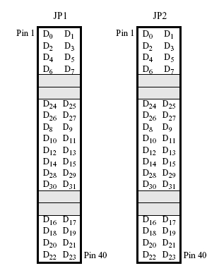
On the DE2 board there are two PIT devices called GPIO 1 and GPIO 2. Each provides 32 external connections named as D0 through D31. These connections are called General Purpose I/O pins because each is a single wire which can be used as digital input or output. Under program control we can either read the logical level at each of those wires (i.e., whether the voltage on that wire is a logical 1 or a logical 0) or set their voltage to logical 0 or logical 1. Physically the GPIO pins appear on the JP1 and JP2 connectors on the boards. Here’s a diagram of how the pins are connected (the gray boxes correspond to pins that are not used by the port – they are connected to the power supply rails):
As an example we will consider an application where the PIT is used to control the fan of a heating system. The PIT will be used to read the status of a thermostat and then it will be used to turn on or off the heating system’s fan. We will assume that the thermostat provides a single output which is 0 if the temperature is less than a preset level and 1 otherwise. We want to turn on the fan if the thermostat’s output is 0 and turn it off otherwise (you may observe that a computer is probably an overkill for this application, however, please recall this is an example). So, one of eight PIT connections will be used as input to read the thermostat status and another will be used as output to control the fan motor.
The PIT interface presents a programming interface that consists of two bytes in memory (there are more registers which we will describe later on). For port GPIO 1 the two registers are:
The DATA register (DR) at address 0x10000060 (read or write)
The DATA DIRECTION register (DIR) at address 0x10000060 + 4 = 0x10000064 (read or write)
|
Address |
WORD |
|
|
0x10000060 |
DR |
Data Register |
|
0x10000064 |
DIR |
Direction Register |
We can view the device as having a base address of 0x10000060, and the two registers at offsets (distances) +0 for DR and +4 for DIR. The other PIT is identical using only a different base address. Here’s the complete list:
1. PIT 1: 0x10000060
2. PIT 2: 0x10000070
In addition to the two registers we just described each PIT has two more registers which are used to control the port’s interrupt behavior. More on this when we start discussing interrupts.
As we noted earlier the PIT provides 32 external single “bit” (wire) connections to the outside world.
Each of these connections can be configured as an input or an output independently. This can be done by writing a value into the DIR register. The DIR register has 32 bits which we can change by storing a word into the address where DIR is mapped at. Each of these bits controls the direction of the corresponding external connection. For example, if bit 0 of DIR is set to 1, then D0 becomes an output otherwise it becomes an input. When we access an I/O device we *have* to use the IO variants of loads and stores, e.g., ldwio or stwio. These instructions bypass any temporary buffering that the CPU may be performing and send the memory requests immediately.
Here are a couple of example of configuring the PIT ports for input or output:
Configure all pins as outputs
addi r8, r0, 0xFFFFFFFF
movia r9, 0x10000064
stwio r8, 0(r9)
Configure all pins as inputs
addi r8, r0, 0
movia r9, 0x10000064
stwio r8, 0(r9)
Configure pins D0 through D3 as outputs, and pins D4 through D31 as inputs
addi r8, r0, 0x000000F
movia r9, 0x10000064
stwio r8, 0(r9)
To set the value of a PIT bit to a specific level we have to write the
corresponding bit of the DR register. Thus, assuming that DIR=0xFFFFFFFF, then
writing 0x0000000F into DR forces D0-D3 to logical 1 and D4-D31 to logical 0.
If a pin is configured as an input, writing the corresponding DR bit does not
change the pin’s value. Such writes are silently ignored.
At any time we can read the DR register and read the logical values of the 32 external connections. If a connection has been configured as an output we are effectively reading the value we have written in the corresponding DR bit. If a connection has been configured as an input then we are directly reading whatever value has been placed on the connection from the outside world (for example from the thermostat).
Example: Let’s us now write the program that reads the thermostat and controls the heating fan. We will assume that the thermostat is connected to bit 0 of PIT 1 (which should be configured as an input) whereas the fan is connected to bit 2 (which should be configured as an output). The thermostat outputs 0 when it’s cold and we need to turn the fan on, otherwise it outputs 1.
So:
D0 is connected to the thermostat’s output
D2 is connected to the heat fan motor
PIT_DR_OFFSET equ, 0x0 # So, DR is at PIT1_BASE + PIT_DR_OFFSET
PIT_DIR_OFFSET equ, 0x4 # and, DIR at PIT1_BASE + PIT_DIR_OFFSET
.text
heat:
movia r9, PIT1_BASE
addi r8, r0, 4
stwio r8, PIT_DIR_OFFSET(r9) # configure all pins but D2 as inputs
stwio r0, PIT_DR_OFFSET(r9) # turn off the motor
fever:
ldwio PIT_DR_OFFSET(r9), r8 # read all pins
andi r8, r8, 0x1 # mask out all but D0
beq r8, r0, fanon # if zero, then it’s cold turn the fan on
fanoff:
stwio r0, PIT_DR_OFFSET(r9) # turn fan off or keep it off
br fever
fanon:
addi r8, r0, 4
stwio r8, PIT_DR_OFFSET(r9) # turn fan on or keep it on
br fever
In order not to forget that C provides us with most of the functionality that assembly does, here’s how the aforementioned code can also be written directly in C:
#define DR ((unsigned int *) 0x10000060)
#define DIR ((unsigned int *) 0x10000064)
void
heat (void)
{
unsigned int t;
*DIR = 0x4;
*DR = 0x0;
while (1)
{
t = *DIR;
if (t & 0x1)
*DR = 0x0;
else *DR = 0x4;
}
}
So, while programming try to avoid using assembly as much as possible. In most cases this will be possible. However, there are cases where using assembly will be important and necessary (for example, you have little control of how the compiler translates a piece of C code, hence it may use inefficient instruction sequences, moreover, since the compiler does not have an understanding of device semantics – programming model – it may use instruction sequences that have unexpected behavior such as accessing the same device register multiple times).
A cleaner/easier to read way of implementing the code in C uses a structure declaration for the device:
struct PIT_t {
unsigned int DR;
unsigned int DIR;
};
struct PIT_t *pitp = ((struct PIT_t *) 0x10000060)
void
heat (void)
{
unsigned int t;
pitp->DIR = 0x4;
pitp->DR = 0x0;
while (1)
{
t = pitp->DR;
if (t & 0x1)
pitp->DR = 0x0;
else pitp->DR = 0x4;
}
}
In this code we exploit the fact that the structure elements are laid out in memory one after the one. So, the DR element appears first, occupying four bytes. Immediately, after it is DIR. This style is easier to maintain and exposes the true structure of the device. We can now use the structure to refer to the other PIT devices easily. Otherwise, we would have to write the addresses of each register explicitly every time. With the structures we only need to write the base address of each device. This style is easier to maintain also. In the documentation for the NIOS II system we use, you will see that the PIT has a couple more registers. We can expand the structure definition once to include these registers without having to change the code much.
Another Example – Debouncing
As an additional example let us consider what happens when the thermostat uses a mechanical arrangement where metal contacts touch to report a logical 1. Whenever metal contacts are used there is a short period of time where they bounce repeatedly whenever the switch changes state. So for a short period of time what we will observe at thermostat’s output will be a series of alternating 0’s and 1’s. The NIOS II is much faster in processing instructions hence the above code will turn on and off the fan several times while the thermostat changes state. We can revise our program to reduce this or even avoid it completely. This is typically called debouncing. Here’s one way of achieving this: Rather than reading the DR once (taking a single sample of the input’s state) we read it several times counting how many times it was 1. If we took N samples and the number of those samples that was one is greater than N/2 then we can assume that the value read is 1 otherwise we can assume it is a zero. Here’s the code:
PIT1_BASE equ, 0x10000064
PIT_DR_OFFSET equ, 0x0
PIT_DIR_OFFSET equ, 0x4
.text
heat:
movia r9, PIT1_BASE
addi r8, r0, 4
stwio r8, PIT_DIR_OFFSET(r9) # configure all pins but D2 as inputs, D2 controls the fan motor
stwio r0, PIT_DR_OFFSET(r9) # turn off the motor
fever:
addi r10, r0, 1000 # we’ll be taking a 1000 samples in r11
add r11, r0, r0 # r11 = 0
sampling:
ldwio r8, PIT_DR_OFFSET(r9) # read all pins
andi r8, r8, 0x1 # mask out all but D0, DO is the thermostat
add r11, r11, r8 # r11 = r11 + bit 0 of DR, or equivalenty if (D0 == 1) r11 = r11 +1
subi r10, r10, 1 # r10 = r10 – 1, one fewer sample needed
bne r10, r0, sampling # more samples needed
addi r10, r10, 500 # 500 is the threshold
bgt r11, r10, fanon # if more than a 500 ones turn the fan on
fanoff:
stwio r0, PIT_DR_OFFSET(r9) # turn fan off or keep it off
br fever
fanon:
addi r8, r0, 4
stwio r8, PIT_DR_OFFSET(r9) # turn fan on or keep it on\
br fever
Please note that I have not tested this code on the DE2 so, using 1000 may not
be the best possible choice or even a good one.
The PIT Implementation
The example in this section shows a PIT with 8 external
connections. Its DR register appears at location 0xFF1110 and its DIR register at location 0xFF1114. From this
description you should be able to make the necessary changes to create a 32-bit
PIT at the addresses used on our system.
Having seen how to program the PIT we can now discuss one implementation. This is not necessarily how it is implemented on the DE2. At the physical level the PIT presents the following signals:
Data: a set of 8 wires that are used for supplying the value to written to registers DIR or DR, or to read the value from the DR. These signals can be used as input or as output as explained subsequently.
A DIR write
signal: When this is 1 the value in the Data is written into the DIR
What appears to software as a single register DR is implemented using separate elements for input and output. The DRO latch implements the output portion, while a tri-state buffer is used for the input portion. Here’s the diagram of one PIT bit:
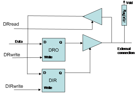
The DRO and DIR boxes are latches. We can change their value using the Data and Write signals. The DIR latch output drives a tri-state driver whose output is connected to the external connection. If DIR is 1 then the tri-state buffer behaves like a buffer and passes the value of the DRO latch to the external connection. If DIR is 0 then the tri-state buffer is placed in the off state which can be thought as an open switch (no connection). In this case, an external source will determine what the value is on the external connection wire. The resistor is there to help when DRO wants to drive a 1 (high voltage) since the technology used is not very “strong” when driving a one. The registor also sets the external connection to 1 when no one is driving it.
If DR Read becomes 1 then the upper tri-state buffer is activated and passes the value on the external connection to the data wire. What we have described is just one of the 8 slices used by the PIT. The 8 slices are connected together so that they share the Write and Read lines and so that their data lines collectively form the 8-bit data interface of the PIT.
To connect the PIT to the NIOS II processor we need to first explain what is the physical memory interface. This discussion follows. We do not discuss the exact implementation of NIOS II. Instead we present an interface that is simple enough to allow us to focus on the fundamentals.
Memory
------------------------------------------------------------------------------------
And in order to not forget that we eventually we will be talking about actual implementations let’s see how a typical memory interface will look at the physical level. This exercise will allow us to see how we can use the binary system to encode quantities other than numbers.
So, let’s start first with the vocabulary we need to be able to talk. This includes the operations and their arguments. Our goal is here to determine how many signals (i.e., bits) we will need to be able to specific these operations. We have the following operations:
Load.DataType Address
Store.DataType Data, Address
Where DataType can be any of the following three: byte, word or long-word. Address is 24 bits for 64k. And Data can be 8, 16 or 32 bits.
These requirements can be stated as follows:
Two operations: load or store
Three data types: byte, half-word or word
One address of 32 bits
One data value of at *most* 32 bits for specifying the value to write for stores
One data value of at *most* 32 bits for memory to returns the value for loads
We also need to be able to say that we do not want to read or write from/to memory, i.e., do nothing
For 1 it’s enough to use a single signal which we will call R/W’. When R/W’ = 1 then we want to perform a load, while when R/W’ = 0.
For 2, it’s enough to use two signals. Let’s call them collectively DW and use the following encoding (others possible):
DW | Data Type
----------------
00 | byte
01 | half-word
10 | not used
11 | long-word
For 3 and 4 we need 32 signals for each (or we could multiplex the same wires).
Finally for 5 we need a master-enable signal ME. When ME = 0 memory ignores all other signals. When ME = 1 then memory looks at the other signals and responds accordingly.
Besides being able to say to memory “do noting” ME plays another important role. In the physical world it takes time for us to setup coherent values on all signals. For example, assume we want to perform in sequence a STORE.BYTE 0x10, 0X000000 and a STORE.BYTE 0x01, 0xffffff. It is practically impossible to change all signals instantaneously. So, in going from address 0x000000 to 0xffffff all possible binary numbers may temporarily appear (because different signals may change at different rates). Without the ME, the memory could get confused and misinterpret the second store. With ME, we can se ME to zero in between the two stores, wait sufficient time for the second store values to appear on the data and address signals and then set ME=1. This way memory remains oblivious to temporarily inconsistent values.
Connecting the PIT to the Memory Interface
----------------------------------------------------------------------------------------------------
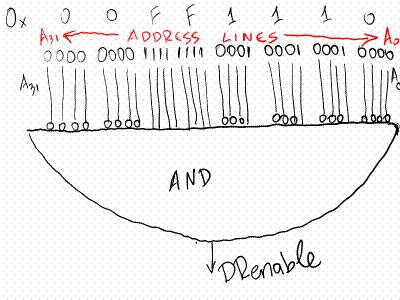
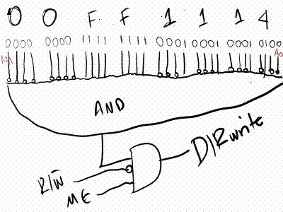
To connect the PIT to the memory interface described previously, we first connect the PIT Data lines to the lower byte (8 bits) of the memory data lines. This will allow us to access the three PIT elements (DIR, DRO and DRI) by using load and store memory accesses. Then we need to activate the corresponding PIT elements depending on the address accessed. We need to detect the following combinations on the address lines: 0xFF1110, and 0xFF1114. In the simplest to describe implementation we use a 32 input AND gate for each of those. Let’s see how we decode the address 0x00FF1110. Using a 32-bit input here’s how we can detect this combination on the address lines: write the number in binary. For every digit that is 1 connect the corresponding wire directly to the AND gate. For every digit that is 0, connect the corresponding wire first to inverter and then connect the output of the inverted to the AND gate.
Here’s the ADDRESS DECODING part for DR, it generate the signal DRenable that tells us that the processor is either reading or writing DR:
DRenable can now be combined with R/W’ and ME to generate the DRread and DRwrite signals:
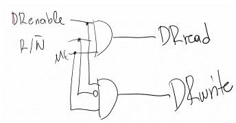
Here’s the address decoding and signal generation circuit for DIRwrite:
In total we used two three 32-input AND gates and three 3-input AND gates. Each of the two 32-input AND gates is connected to all 32 address signals. By using inverters appropriately we can detect that the address being accessed is one of those mapped to DR, and DIR. We start by looking at the binary representation of these addresses and put an inverter for those address bits that are zero in the pattern we are interested in. After detecting the address, we then used a 3-input AND gate to detect accordingly whether an access is being made (ME == 1 – ME is Master Enable), and whether it is a read or a write.
This implementation is easy to understand, however, it’s not necessarily the most efficient. This topic is beyond the scope of this lecture, however, you are encouraged to think of ways of reducing the number of components needed to do address decoding.
Here’s the complete design:
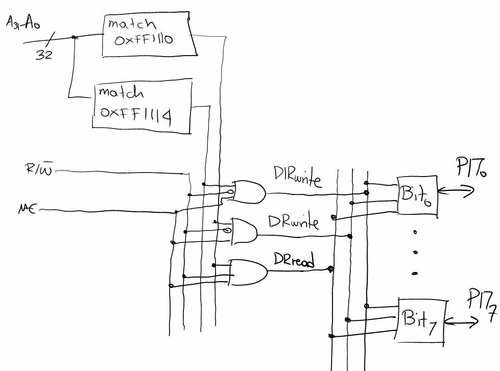
Each
bit cell (there are eight of them) is as shown earlier). The boxes labeled
“match some hex value” are the 32-bit input AND gates we described earlier.