Computer Organization
Multi-Cycle Implementation: The Control Unit
Andreas Moshovos
Spring 2005
In the previous lecture we have explained the datapath of the multi-cycle implementation. Here we present the design methodology and the design for the control unit.
For the single-cycle implementation the control was a combinatorial circuit. For the multi-cycle implementation the control is no longer a combinatorial circuit, it’s a finite state machine.
Here’s why: It takes multiple cycles to execute an instruction. During each cycle different actions will have to take place. The actions depend not only on the instruction but on which cycle this is. So, for an ADD different things happen depending on whether we are at cycle 2 or 3. Accordingly, a circuit that can keep track of which cycle we are in is necessary.
To design the control we start by producing a table that lists all the actions that need to take place per cycle and per instruction:
|
CYCLE |
Instruction
Class |
|||||||
|
|
ADD, SUB,
NAND |
SHIFT |
ORI |
LOAD |
STORE |
BPZ |
BZ |
BNZ |
|
1 |
[IR] = Mem[ [PC] ] [PC] = [PC] + 1 |
|||||||
|
2 |
[OpA] = RF[ [IR7..6] ] [OpB] = RF[ [IR5..4] ] |
|||||||
|
3 |
[ALUout] = [OpA] op [OpB] |
[ALUout] = [OpA] shift Imm3 |
[OpA] = RF [1] |
[MDR] = Mem[ [OpB] ] |
MEM[[OpB] = [OpA] |
if (N’) PC = PC + SE(Imm4) |
if (Z) PC = PC + SE(Imm4) |
if (‘Z) PC = PC + SE(Imm4) |
|
4 |
RF[ [IR7..6] ] = [ALUout] |
[ALUout] = [OpA] OR Imm5 |
RF[[IR7..6]] = [MDR] |
|
|
|
|
|
|
5 |
|
|
RF[ 1 ] = [ALUout] |
|
|
|
|
|
We now use this table as guide in constructing the state diagram for the control finite state machine:
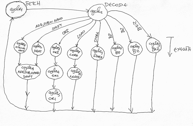
Instruction execution starts at state “cycle1”, this where we will be fetching the instruction opcode from memory.
In the next state “cycle2” we read from the register file and also have the control decode the instruction.
Past state “cycle2” different actions take place depending on the instruction opcode. The labels on top of the arrows refer to different instructions. At the physical level these are the values on the IR bits 0 through 3. These four bits hold the instruction opcode (e.g., 0000 for load, 0100 for add and so on).
Note that we were able to merge the state for cycle 4 for instructions ADD, SUB, NAND and SHIFT since they all perform the same action at that cycle. This is an optimization.
So we have the beginnings of a control finite state machine. The next step is determining what values the various datapath control signals (like RegWrite) should take at each state.
Given an understanding of the datapath and of the actions that need to take place at each state this process is straightforward. Let’s start by determining what values the control signals should take at each state:
“CYCLE1”: Fetching an instruction and incrementing the PC (row
“cycle1” in the aforementioned table)
We have determined before that the following actions take place during this state:
|
CYCLE |
Instruction
Class |
|||||||
|
|
ADD, SUB,
NAND |
SHIFT |
ORI |
LOAD |
STORE |
BP |
BZ |
BNZ |
|
1 |
[IR] = Mem[ [PC] ] [PC] = [PC] + 1 |
|||||||
With this as guide we now determine the values for all datapath control signals (check the lecture on the datapath to recall what each signal does):
PCWrite = 1 à since we do want to write PC + 1 into the PC
AddrSel = 1 à we want to use the PC’s value to drive the address lines of memory
MemRead = 1 à we want to read from memory
MemWrite = 0 à we do not wish to write to memory
IRLoad = 1 à we do want to write the value read from memory into IR
OpASel = X à we do not care what gets read from the register file
MDRload = X à we are not using MDR so it could change with no harm
OpABLoad = 0 à we do not wish to change register OpA and OpB (this signal is not listed on the datapath diagram but it is connected to the temporary registers OpA and OpB and controls whether they load the values read from the register file. We could have used X here as it would have been safe to change these registers now.
ALU1 = 0 à we do care what is the first input to the ALU as we want to calculate PC + 1.
ALU2 = 001 à we want the constant 1 as our second ALU input to calculate PC + 1.
ALUop = 000 à we want to do addition
RFWrite = 0 à we do not want to write into the register file. Note that this cannot be X since we do not wish to write and writes are irreversible.
RegIn = X à we are not writing into the register file
ALUOutWrite = X à we do not care if the temporary register ALUOut is changed
FlagWrite = 0 à we need to retain the value of the flags
“CYCLE2”: Decoding the instruction and reading from the register
file
We have determined before that the following actions take place during this state:
|
CYCLE |
Instruction
Class |
|||||||
|
|
ADD, SUB,
NAND |
SHIFT |
ORI |
LOAD |
STORE |
BP |
BZ |
BNZ |
|
2 |
[OpA] = RF[ [IR7..6] ] [OpB] = RF[ [IR5..4] ] |
|||||||
With this as guide we now determine the values for all datapath control signals (check the lecture on the datapath to recall what each signal does):
PCWrite = 0 à since we do not want change the PC
AddrSel = X à we will not be accessing memory, so any address is fine
MemRead = 0 à we do not want to read from memory
MemWrite = 0 à we do not wish to write to memory
IRLoad = 0 à we do not want to change the IR
OpASel = 0 à we do care what gets read from the register file, we want the OpA field from the instruction stored in IR
MDRload = X à we are not using MDR so it could change with no harm
OpABLoad = 1 à we do wish to change register OpA and OpB
ALU1 = X à we do not care what is the first input to the ALU.
ALU2 = XXX à we do not care what is the first input to the ALU.
ALUop = XXX à we do not care what calculation the ALU does
RFWrite = 0 à we do not want to write into the register file.
RegIn = X à we are not writing into the register file
ALUOutWrite = X à we do not care if the temporary register ALUOut is changed
FlagWrite = 0 à retain the flag values
Continuing along these lines we will end up with a
complete description of all datapath control signals
per state. We this information we can now have a complete finite state diagram
assuming a Moore-style implementation (
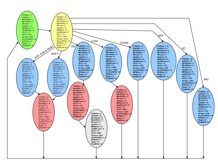
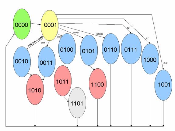
This is the complete state transition diagram for our control finite state machine. All that remains is assigning binary values to states, writing the state transition table and then designing the circuit as we would any other finite state machine.
In total there are 14 states. Thus we need a four bit number to represent each state.
The state transition table will have the current state and instruction opcode as inputs. As outputs it will have the next state and the values that the control signals take during that state (signals listed inside the states in the previous diagram).
The control will look as follows:
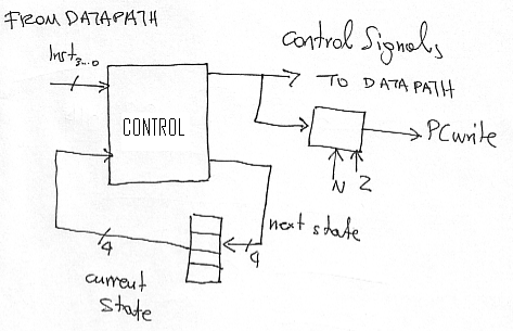
It accepts the IR3..0 signals from the datapath (from the IR register) and the current state as this is encoded in four flip-flops. Every cycle it produces values for the control signals which are sent to the datapath. The PCWrite signal also needs to take into account the values of N and Z. This is why an additional combinatorial circuit is needed. We could have provided different states for each branch depending on the values of Z and N.
Here’s the state transition table (it includes only the next state and not the control signals as the latter do not depend on the transitions but only on the current state):
|
INPUTS |
OUTPUT |
|
|
|
IR3..0 |
|
|
0000 (Cycle 1) |
XXXX |
0001 |
|
0001 (Cycle 2) |
0000 (load) |
0101 (load cycle 3) |
|
0001 |
0001 (store) |
0110 (store cycle 3) |
|
0001 |
0100 (add) |
0010 (add/sub/nand cycle 3) |
|
0001 |
0110 (sub) |
0010 |
|
0001 |
1000 (nand) |
0010 |
|
0001 |
X111 (ori) |
0100 (ori cycle 3) |
|
0001 |
X011 (shift) |
0011 (shift cycle 3) |
|
0001 |
0101 (bz) |
1000 (bz cycle 3) |
|
0001 |
1001 (bnz) |
1001 (bnz cycle 3) |
|
0001 |
1101 (bpz) |
0111 (bpz cycle 3) |
|
0010 (add/sub/nand cycle 3) |
XXXX |
1010 (add/sub/nand/shift cycle 4) |
|
0011 (shift cycle 3) |
XXXX |
1010 (add/sub/nand/shift cycle 4) |
|
0100 (ori cycle 3) |
XXXX |
1011 (ori cycle 4) |
|
0101 (load cycle 3) |
XXXX |
1100 (load cycle 4) |
|
0110 (store cycle 3) |
XXXX |
0000 (next instruction) |
|
0111 (bp cycle 3) |
XXXX |
0000 |
|
1000 (bz cycle 3) |
XXXX |
0000 |
|
1001 (bnz cycle 3) |
XXXX |
0000 |
|
1010 (add/sub/nand/shift cycle 4) |
XXXX |
0000 |
|
1011 (ori cycle 4) |
XXXX |
1100 (ori cycle 5) |
|
1100 (load cycle 4) |
XXXX |
0000 |
|
1101 (ori cycle 5) |
XXXX |
0000 |
|
1110 (unused) |
XXXX |
0000 (go to state 0) |
|
1111 (unused) |
XXXX |
0000 |
Where we used the following encoding of states:
This finite state machine can be designed with the methodologies described during the digital design course. We have to pick a flip-flop (D, J-K, RS or T) and then derive the functions that will drive the flip-flop inputs so that the specified transitions will happen.
In order to design the circuit that generates the control signals we will have to draw the truth table. The input here will be the current state (and the Z and N bits) and the outputs are those specified in the state diagram that we presented earlier. So, our truth table will have a single line per state and Z/N combination and as outputs will list all control signals.
After this table is filled in designing the corresponding circuit is straightforward. This is combinatorial circuit hence the methodologies you learned during the digital design course apply.