Department of Electrical and Computer Engineering
ECE 241F Digital Systems, Fall 1996
Lab #1
Purpose: The purpose of this lab is to familiarize you with the equipment in the digital laborartory, which you will be using heavily for all labs and the project. It will also the first chance to build some basic combinational and sequential logic.
Background: During the hardware labs, you will be using some equipment developed by this Department. Although the equipment is quite robust and easy to use, we advise you to read this text first and handle the equipment carefully.
Preparation: Read through this document and do the preparation in part 4b below.
1. Information about basic equipment. Read the sections a-d below and find each of the described equipment pieces.
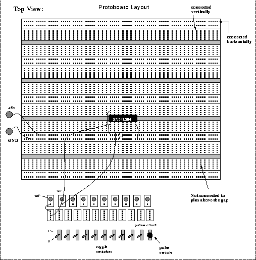
a. Protoboard: The protoboard and switch board are integrated on the board that also has the power supply. The schematic of the protoboard is given in the figure below. The wiring channels run either horizontally or vertically. The horizontal channels are primarily used for distributing power and the vertical channels are used for connecting the wires together and connecting to the chips. Signals are generated on the switching board by switches, a clock generator, and a single-pulse generator.
b. Logic probe: The logic probe, attached to each protoboard tells you the digital value of any signal. We will be mostly using the TTL signal levels, hence the corresponding setting on the probe should be selected. Touch the probe to +5V and ground on the protoboard to observe what it does for high and low. There is also a separate switch on the probe for detecting oscillating signals, as well as pulses. Try to select that switch and connect the probe to the output of the clock. Observe what happens. Repeat the same thing with the pulse switch turned off.
c. Chip puller: To preserve the chips, and in the worst case, to avoid mangled fingers, everyone should use the chip puller when removing chips from the board. Practice inserting and removing one of the 7400-series TTL chips.
d. Strippers, cutters are attached to the board for your convenience.
2. Chips: The majority of chips used in the laboratory are medium speed IC's of the 74XX TTL logic family. The pin configuration of a 14-pin dual in-line chip is shown as an example.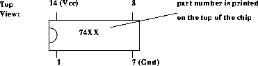
Each chip has to have a source of power to function properly. For 74XX logic family pin 14 is connected to Vcc = + 5V and pin 7 is grounded.
3. Wiring procedure: Based on the specification sheets of the chips used assign each gate of your circuit diagram a package label and then enter all relevant pin numbers on the circuit diagram, as indicated below. For example, package X is a 7400, and package Y is a 7402. Each distinct chip should have its own label. Your package list will tell you what chip types you need and how many. 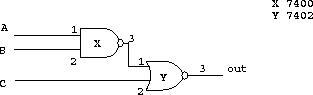
With the power switch in the "off" position, wire the circuit on the protoboard. Recheck the wiring (if in doubt, ask for assistance), then switch the power switch "on" and demonstrate that the circuit works as expected.
4. Circuit building practice.
a. Build and test the circuit that is equivalent to the circuit shown in Figure 1 of LogicWorks Exercise #1. Recall that it was designed using a minimum number of NAND gates. For your preparation, you should produce a properly labeled schematic.
b. Preparation: Investigate, explain and simulate the operation of the two feedback circuits shown in the figure below. Under some conditions, the circuits will oscillate. What are these, and how can you show this situation by the simulator?
c. Experiment: Build and test each circuit on the protoboard. Use two LED's to show the states of the two outputs, Q and Q', for various input sequences. Produce the state tables that describe the operation of each of the circuits. 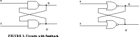
Generated with WebMaker