P. Chow and J. Rose
Fall 1996
The purpose of the lab is to understand operation of flip-flops, counters and ring oscillators. You will uses the different parts of this lab to make an actual measurement of the propagation delay of a basic logic gate.
Each of the following sections gets you to build a part of a rather large circuit that you will use at the end to measure the delay of a basic logic gate.
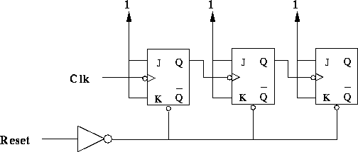
Figure 1: A 3-bit ripple counter.
Notice that after the Reset signal goes low, the counter is enabled and begins to count. It is often useful to have counters that count up to a specific value and then stop. Design a modification of this counter circuit such that the counter stops counting when it reaches the value 4. (In another part of this lab, we will ask you to make a counter that stops at a different number, so try to come up with a scheme for doing this which you can apply to any stop-count number) The counter should stay at this value until the counter is Reset again. Note the following:
Build and test this circuit, first by clocking it manually. Then connect it to the oscillator provided in your laboratory setup.
Note: When building this circuit, you will have some unused inputs. What can happen if you leave them floating (unconnected)? What is the solution?
Preparation: Enter and Simulate your N=4 counter circuit using LogicWorks. Bring the schematic and simulation printouts. Answer the above question.
Build this circuit. Do not disassemble this circuit. You will need it for PART II.
Preparation: Enter and Simulate your circuit.
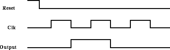
Figure 2: Timing of the desired output.
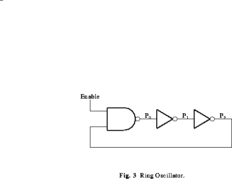
Review of Ring Oscillators
In an earlier lecture we discussed the operation of a Ring Oscillator, as illustrated in Figure 3. The following discussion reviews the operation of that circuit.
The circuit shown consists of three inverting gates
connected in a ring. While the Enable input is equal to 0, points
![]() , and
, and ![]() will be at logic levels 1, 0
and 1, respectively. Consider what happens when Enable is changed
from 0 to 1. The state at point
will be at logic levels 1, 0
and 1, respectively. Consider what happens when Enable is changed
from 0 to 1. The state at point ![]() is given by:
is given by:
![]() =
= ![]()
Because of the propagation delay through the gate, the state of
![]() at time t is actually a function of the state of the gate
inputs at time
at time t is actually a function of the state of the gate
inputs at time ![]() , where
, where ![]() is the propagation delay
through
the gate.
That is:
is the propagation delay
through
the gate.
That is:
![]() =
= ![]()
Hence, after one gate delay from the moment Enable becomes equal to 1,
![]() becomes equal to 0. One gate delay later,
becomes equal to 0. One gate delay later, ![]() changes
to 1, and so on. Let
changes
to 1, and so on. Let ![]() be the instant at which Enable changes
from 0 to 1. The sequence of events may be described as follows:
be the instant at which Enable changes
from 0 to 1. The sequence of events may be described as follows:
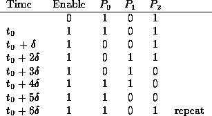
This sequence of events will repeat indefinitely, producing
oscillatory signals at ![]() , and
, and ![]() .
.
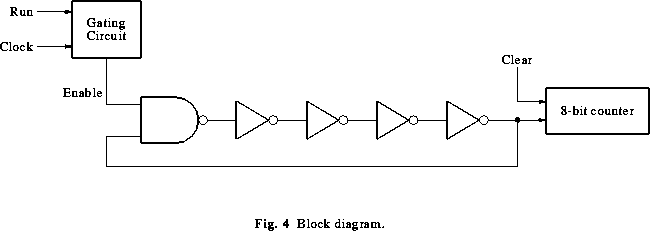
Lab Exercise
The purpose of this part of the lab is to use
the ring oscillator to measure the gate propagation
delay, ![]() , by measuring the oscillator's frequency. Design and build
a circuit, given in block diagram in Figure 4, to do so as follows:
, by measuring the oscillator's frequency. Design and build
a circuit, given in block diagram in Figure 4, to do so as follows:
The required measurements are easily done with the equipment available in the laboratory if you choose the number of gates in the ring, n = 13 and a time period equal to one cycle of the built-in oscillator of your digital board setup. Use two 4-bit counter chips (74LS193) to build an 8-bit counter to count the number of pulses. A block diagram for the required circuit is shown in Figure 4 for n = 5.
Using LogicWorks, first simulate your circuit. The 74193 is available in the 7400 library. It will help you make sure that you have made the correct connections to the chips. You will have to set the delay of the gates in the ring to some value other than the default 1.
You will use the the built-in oscillator in the digital lab board
to provide the input clock. The last page of the handout
for lab #1 tells you how to calculate the period of the
clock as a function of the capacitor attached to its terminals.
When a 10pF timing
capacitor is used,
it has a period of about 20-25 ![]() but the frequency of oscillation may vary from
board to board.
You must also take into account about 20pF of parasitic capacitance
when using the timing period formula given in the handout.
The parasitic capacitance is due to effects such as the protoboard
connections and the wires. This will vary from board to board.
but the frequency of oscillation may vary from
board to board.
You must also take into account about 20pF of parasitic capacitance
when using the timing period formula given in the handout.
The parasitic capacitance is due to effects such as the protoboard
connections and the wires. This will vary from board to board.
Using this set up, measure the propagation delay of the inverters. Do your measurement several times and average the results. Why is this a good practice?
Change your circuit by adding a few more inverters, and redo the measurements.
Preparation: Answer questions 1 to 4 above. Enter and simulate a circuit to do the gate delay measurement, as described above.