University of Toronto
Department of Electrical and Computer Engineering
ECE 241F Digital Systems, Fall 1996
LogicWorks Exercise #1
Objective: To introduce the LogicWorks simulator. By the end of this exercise you should be familiar with:
1. Creating simple schematics.
2. Observing behaviour using timing diagrams.
3. Entering stimulus waveform using timing diagrams.
4. Printing out schematics and timing diagrams.
5. Using the manual.
This exercise should serve as an introduction to Lab #1. Bring the results of this exercise to that lab with you, as it will be checked as part of your preparation.
Note: All page references are to the manual for LogicWorks 3.
1.0 Introduction to Logicworks
1. Install the logicworks software onto your computer, following the instructions on page 13 for Windows machines, and page 18 for Macintosh machines.
2. Read through the "User Interface" chapter, page 27 for Windows and page 37 for Macintosh.
3. Do the "five minute" tutorial on pages 47-63.
4. Read the remainder of chapter 4, which has more useful details on schematic entry and simulation.
2.0 Work
1. Logic Gate Networks.
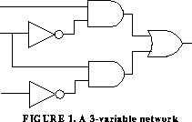
a. Derive the truth table for the logic gate network shown below in Figure 1:
b. Draw the network using the LogicWorks software, specifically using the primgate library. Connect a binary switch (from the primio library) to each input (ref: pg. 55) and a binary probe to the output (ref: pg. 60-61). Test the truth table by setting the switches to all possible combinations.
c. Label the inputs and the output (ref: Naming a signal, pg. 56-57). (Note that if the label is not properly attached, no signal is shown in the timing diagram window.) Repeat the testing as in step b), and observe the timing diagram. To actually make the timing diagram activate, you need to cause an event to happen. An event is the changing of the value of any signal. See page 160 for a discussion of the even-driven nature of the simulator.
d. Draw an equivalent circuit of the network using a minimum number of NAND gates (use 2-input NAND gates only). Show by simulations that the circuit is equivalent to the circuit in Figure 1.
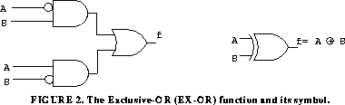
e. The Exclusive-Or (EX-OR) gate network and its symbol are shown in Figure 2. Derive the truth table and implement the circuit using as few NAND gates as possible. Can you get it down to four gates? Use the LogicWorks software to show that the two circuits are equivalent.
f. Design a network that checks simultaneously if the circuit in Figure 1 and its minimal NAND implementation perform the same function. The network should have a single output. The output of the checking circuit is one if the two circuits are not the same. Show by simulations that the output is 0 for all possible input combinations.
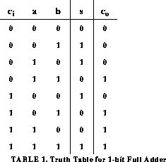
2. Binary Adder
Table 1 gives the truth table for a one-bit binary full adder, illustrated in Figure 3. Give a suitable implementation for this circuit. Extend your design to build a 2-bit adder using EX-OR and NAND gates. Test the designed circuits using the LogicWorks software. You should try using the option of entering the stimulus waveforms on the timing diagram. Print the schematic and the timing diagram.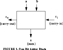
Generated with WebMaker