ECE241F - Digital Systems - Lab 2
Quartus II CAD Software Tutorial and Use
Fall
2003 J. Rose, B. Wang
1.0
Purpose
The purpose of
this lab is to learn the basics of the CAD design software we’ll use throughout
the course: design entry using schematics and the Verilog hardware description
language, simulating your circuit on a computer to determine if the design is
correct and automatic synthesis to create the working circuit in the lab. It
will also introduce a large-scale programmable logic device, and show you how
to download a circuit into the device. Warning:
there are many new concepts and things to do in this lab! Don’t worry if it doesn’t make sense the
first time around; you’ll be surpised about how naturally it will all come to
you by the end of the course.
2.0 Preparation
1.
The first task is to become
famliar with the Altera Quartus II version 3.0 CAD software. You’ll need access
to that software as described in the software
handout (note that your EECG ugsparc computer login name and password will be
the same as your ECF password; if you don’t have an ECF password, go see the
ECF Administration in the Engineering Annex, Second Floor ).
i. Do Tutorial #1 (labelled
“Appendix B, Tutorial 1 – Using Quartus II CAD Software”) that was given as a
handout and is also located at http://www.eecg.toronto.edu/~zvonko/AppendixB_quartus.pdf.
ii. Do Tutorial # 2 (labelled
“Appendix C, Tutorial 2 – Implementing Circuits in Altera Devices”) that was
given as a handout and is also located at http://www.eecg.toronto.edu/~zvonko/AppendixC_quartus.pdf
Do not do Section C.2, it is
un-necessary. Tutorial sections C.1 and C.4 are to be done before the lab period as
part of the preparation, while section C.3 describes how to actually
program a chip, which you will do during the lab, as described below.
2.
Design, enter and
simulate a circuit, using both schematic entry and Verilog as the
design entry method (i.e do it twice, with the two methods), that implements
the following logic function:
You are to design two functions, f1 and f2,
with four inputs named a, b, c and d. The function f1 should be 1
when a = c and b = d. Otherwise, f1
should be 0. The function f2 should be 1 when the number of 1’s in a, b, c
and d is odd. (That is, count the
number of 1’s in the four variables; if
the count is odd, then f2 is 1, otherwise it is 0.)
Give the truth tables for functions f1 and f2.
Derive a Boolean expression in canonical sum-of-products (i.e. sum of min-terms
only) form for each function. Use algebraic manipulation to simplify the
expressions. Enter the simplified Boolean expressions into Quartus
II in two different ways:
i.
Draw a schematic that includes
the logic gates for both f1 and f2.
ii.
Write Verilog code that
represents both f1 and f2 with Boolean equations.
Your preparation, to be marked, should consist of the printed schematic, the Verilog
code, and the simulator output for all circuits, including that from Tutorial
#1. YOUR PREPARATION MUST BE PRINTED BEFORE THE LAB BEGINS.
2.
You mus either place all your
design files on your home directory on the ECE ugsparcs computers, or bring in
a floppy disk containing your files. Your login name for the ECE ugsparcs is
the same as your ECF account. The password is the same as your ECF password. If
you don’t have either an ECF account or an ECE account, request one from ECF
(in Engineering Annex 2nd floor) and then send a request to tim@eecg.utoronto.ca
to create an ECE ugsparcs account. The ECE ugsparc machines are named
ugsparcXX.eecg.toronto.edu where valid XX numbers are 51-100, 131-180 and
200-252. The machines are located in the south corridor of the Galbraith
building, second floor, rooms GB 243 and GB 251.
3.0 In the Lab
You will need the
information contained in Section 4, below.
1.
Download and test the circuit
of Tutorial #1, as described in Tutorial #2 and Section below. You should be sure to choose pins on
the 7128 device that are available in the Table on page 4 of this handout.
Demonstrate that your circuit works to a TA.
2.
Download and test your circuit
from part 2 of the preparation, and show it to a TA.
4. 0 PC Information for the
Machines in Bahen 3135, 3145, 3155 and 3165 labs.
This section
tells you how to access the files you have placed on the ECE ugsparc machines
from the PCs in the labs in Rooms Bahen 3135, 3145, 3155 and 3165.
1.
Logging in to
get your ECE ugsparc files attached to the PC. Turn on the PC and monitor. The PC should be showing you a login prompt. If not, reboot it using the Start
menu in the lower left hand corner, by selecting the “shutdown” menu item.
Make sure that the “domain” you log into is selected as Gizmo. Your
login name is the same as the ECF and ECE ugsparc login, and your initial
password is your 9 digit student number (change this right away). Your ECE
ugsparc home directory will be mapped to the W: drive. You should be able to see all of the files
you have placed there.
2.
Start the
Quartus II 3.0 program by opening the “Courseware” directory and
double-clicking on the Quartus II 3.0 icon. It will take
less than a minute to load.
3.
With Quartus II running, you
can open your project and compile your design as described in Tutorials #1 and
#2. Before programming the actual chips, go to step 4 below. You
will need to specify which pins to use for your inputs and outputs, to make
sure that the pins used are available from the connector (some of the pins are
hard-wired to devices on the UP1 board, and are not connected to the header). The
Table on page 4 lists which pins are
available on the header.
4.
Before downloading your designs
into the board, connect a 60-pin cable from the Altera UP1 board into the
protoboard - a TA will demonstrate this. Be sure to use the
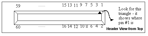
header that is closest to the MAX 7128 device.
Notice that the cable can only plug into the
header one particular way, because the headers have “keys” which prevent
incorrect insertion. The header itself is numbered as follows, as viewed from
the top:
Be sure that the power supply
is switched off.
i.
Connect the power supply to the
Altera UP1 board using the special cable that has a white plastic connector on
one end and a power plug that matches the power-in of the Altera UP-1 board.
ii.
Connect the power supply to the
protoboard as you did in lab #1 using the cable that has the logic probe
attached to it. To Do this, you plug one end into the power supply connector,
and the “banana” plugs into the proto board. You’ll be connecting the ground to
the header in the next step.
iii.
Using diagram above and
Table do the following: first, In
order to make sure there is a good solid common ground between the proto board
and the UP1 board, connecting pin #2 of the header to the ground of the
protoboard. This ensures that the grounds are at the same potential, and so the
switch board and UP1 board have a common reference point.
iv.
Connect your input signals from
the digital switch board to the correct input pins for your circuit on the
protoboard header. You have to check Table below to see the correspondence between the
MAX 7128 chip pins and the header pins. Connect your outputs to digital board
lights in a similar way.
v.
Turn on the power supply.
Download and test your circuit, using the instructions from Tutorial #2,
Section C.3; be sure to have assigned the appropriate pin connections as
described in Tutorial #2, Section C.4
Protoboard
Header - Max 7128 Pin Correspondence
Table 1: Proto-Board Header -
MAX 7128 Pin Correspondence
|
Protoboard Header #
|
MAX 7128 Pin
(or board signal)
|
Protoboard Header #
|
MAX 7128 Pin (or board signal)
|
|
1
|
Raw (beware! don’t use)
|
2
|
Ground
|
|
3
|
Vcc
|
4
|
Ground
|
|
5
|
Vcc
|
6
|
Ground
|
|
7
|
No Connect
|
8
|
No Connect
|
|
9
|
No Connect
|
10
|
No Connect
|
|
11
|
No Connect
|
12
|
GCLRn/1
|
|
13
|
OE1/84
|
14
|
OE2/GCLK2/2
|
|
15
|
4
|
16
|
5
|
|
17
|
6
|
18
|
8
|
|
19
|
9
|
20
|
10
|
|
21
|
11
|
22
|
12
|
|
23
|
15
|
24
|
16
|
|
25
|
17
|
26
|
18
|
|
27
|
20
|
28
|
21
|
|
29
|
22
|
30
|
25
|
|
31
|
24
|
32
|
27
|
|
33
|
29
|
34
|
28
|
|
35
|
31
|
36
|
30
|
|
37
|
33
|
38
|
34
|
|
39
|
35
|
40
|
36
|
|
41
|
37
|
42
|
40
|
|
43
|
39
|
44
|
41
|
|
45
|
44
|
46
|
46
|
|
47
|
45
|
48
|
48
|
|
49
|
50
|
50
|
49
|
|
51
|
52
|
52
|
51
|
|
53
|
54
|
54
|
55
|
|
55
|
56
|
56
|
57
|
|
57
|
Vcc
|
58
|
Ground
|
|
59
|
Vcc
|
60
|
Ground
|