ECE241F - Digital Systems - Lab 3
More Complex Logic Design: 7-Segment Displays
Fall
2003 J. Rose and B.
Wang
1.0 Purpose
The purpose of this lab is to
build several more complex logic circuits and to gain increased familiarity
with the Quartus II 3.0 CAD software.
2.0 Background
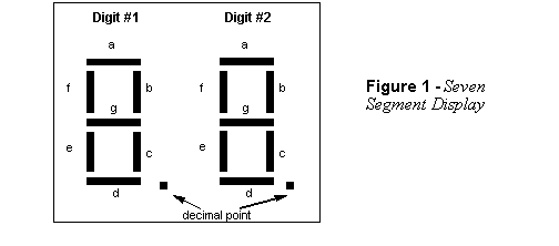
A seven-segment display is often
used on computers, watches, DVD players and many electronic devices to display
numbers and some characters. It consists of seven independent lights (actually
light-emitting diodes (LEDs)) in an “8” configuration as shown below in
Figure 1 on page 3. By turning on different segments, you can
display different numbers and some letters.
3.0 Preparation
You are to create two logic
circuits to drive one of the seven-segment displays on the Altera programmable
logic board. Please see Section 5.0 for details of how to use these
boards. (In particular, note that to turn a light-segment on, you must drive
the corresponding pin to a logical “0”).
Your preparation, to be marked, should consist of the Verilog code and the simulator
output for all circuits. Be sure to print out the simulation results and
Verilog code for marking, and paste it in your lab book.
1.
Design a circuit that takes a four bit (X3, X2, X1, X0) input from the digital switch board (like you did in
Lab #2) and drives digit #1 on the Altera board as described in the table
below. Note that for the letters, some are capitalized and some are not. (The
reason is that a capital B, for example, would come out the same as an 8 on a
7- segment display, so we will display a lower-case b instead).
|
X3
X2 X1X0
|
Display (note the capitalization)
|
|
0000
|
0
|
|
0001
|
1
|
|
0010
|
2
|
|
0011
|
3
|
|
0100
|
4
|
|
0101
|
5
|
|
0110
|
6
|
|
0111
|
7
|
|
1000
|
8
|
|
1001
|
9
|
|
1010
|
A
|
|
1011
|
b
|
|
1100
|
C
|
|
1101
|
d
|
|
1110
|
E
|
|
1111
|
F
|
Determine the equations for the 7-segment display segments, and
minimize them using the Karnaugh-map method described in class. Write Verilog
code to represent the logic function for each segment as a boolean equation
(with AND, OR, NOT, etc.). Simulate and test your equations using the Quartus functional
simulator, or with the timing simulator with the MAX 7128S device set.
2.
Design a similar circuit to the one given in part 1, except
that you should use the four input switches to generate the letters of your
last name. For example, if your last name is Parnas, you could use code 0000 to
display an P, 0001 to display an A, 0010 to display a R (or something as close
to a R as you can get). Note that you can choose any code you wish for each
letter. Notice also that you don’t need to create two codes for a letter that
appears twice in your name. For example, the letter A appears twice in Parnas,
but you only need to produce one code for the letter A - the intent is that you
will be able to spell out your last name on the 7-segment display by entering the
codes for the letters one at a time.
For Fairness: if your last name is
longer than 9 unique letters, you need only do 9 unique characters of
it. If your last name is shorter than 9 characters, you must add more letters
from your first name until you have coded at least 9 unique characters.
Since you will only need to do 9 codes, you can leverage the
don’t cares that will be available in the truth tables.
1.
First, check and make sure that the 7-segment display and
Altera board are working, by copying the file ~jayar/ece241/lab3/flash.pof (on
the ECE ugsparc system) and place it into a separate directory. (You can use
this in all succeeding labs as a quick hardware test).
Then, open a new project (call it flash) in Quartus the Programmer module by selecting Tools |
Programmer, and then select the file flash.pof from your directory using
the Edit|Add File command. You can then download this circuit into the
device in the same way you did in lab #2. The cicuit will count upwards using
the 7-segment displays.
2.
Download and test your circuits from the preparation. Show
each working circuit to the TA.
5.0 Connections Between MAX 7128 and The
Seven-Segment Decoder
The Altera programmable logic
board has two seven segment displays attached directly to the pins of the chip.
The figure below shows the naming of each segment. The subsequent table gives
the connections between segments and the MAX 7128 pins. NOTE:
to turn a segment on, you must drive the associated pin with a “0.” (not a 1).
|
Display Segment
|
7128 Pin for Digit 1
|
7128 Pin for Digit 2
|
|
a
|
58
|
69
|
|
b
|
60
|
70
|
|
c
|
61
|
73
|
|
d
|
63
|
74
|
|
e
|
64
|
76
|
|
f
|
65
|
75
|
|
g
|
67
|
77
|
|
Decimal point
|
68
|
79
|