ECE241F - Digital Systems - Lab 5
Adders and Registers
1.0 Purpose
The purpose of this lab is to introduce the logic needed to create an adder, and use it in combination with registers. The lab also provides practice in coding Verilog and schematic entry.
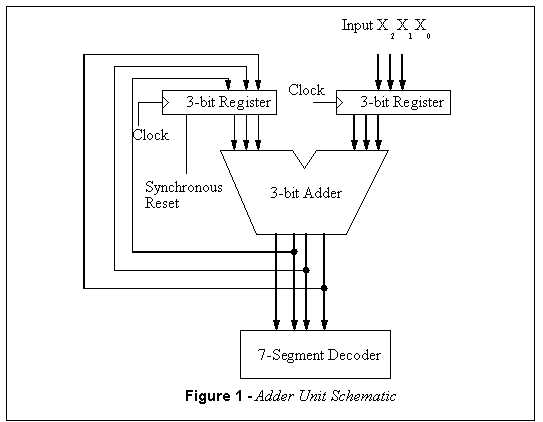
2.0 Background
Using a 3-bit D register with synchronous reset, the seven- segment decoder you built in Lab 3 and an adder unit you’ll build in this lab, you will create a simple arithmetic unit as shown in Figure 1. Its inputs are: a single three-bit binary number (X2X1X0), the clock, and the Reset signal. The four-bit output of the adder is connected to the 7-segment display so that it can be viewed. In the preparation below, you are required to figure out how to use this circuit to add two 3- bit numbers. This is actually a simple version of the arithmetic and logic unit that can be found inside all computers.
|
3.0 Preparation
1. Determine the sequence of control signals and data inputs that you would need to be able to add two 3-bit numbers using the circuit of Figure 1 . You will need to know this in order to properly simulate the circuit that you will be designing. The sequence is essentially a timing diagram (giving the sequence of the input values X2X1X0, Reset and clock) such as you would create using the waveform editor of Quartus to test the circuit. Give the timing diagram for this part of the preparation.
3. Using the adder, two 3-bit D-type registers with synchronous reset, and your seven-segment decoder circuit from Lab 3, build the circuit of Figure 1 using the graphic editor. Simulate your circuit to ensure that it works. SYNCHRONOUS reset of a D register means that the reset doesn’t happen until the next active clock edge. Use the register function available from the Quartus library under megafunctions->storage and select lpm_dff. To customize this “megafunction” use the wizard that pops up to get the right number of bits and the synhcronous reset (clear).
4.0 In The Lab
1. Build and test the adder circuit from part 2 of the preparation.
2. Build and test the register/adder/display unit from part 3 of the preparation.
3. Build and test the register/adder/display unit from part 4 of the preparation.