ECE241F - Digital Systems - Lab 6
Finite State Machines
Fall
2003 J. Rose and B.
Wang
1.0 Purpose
The purpose of
this lab is to become familiar with the design of finite state machines. You
will do three designs: one from “scratch” where you create the entire
circuit schematic for a finite state machine, one using the state machine
specification methods available in Verilog. These first two designs will be
clocked using a manual clock from the digital switch board. The third machine
will be running using the 25MHz on-board clock, and will implement the
handshaking protocol described in class.
You'll use the logic analyzer to watch its behavior.
2.0
Background
In class we have
described a simple state machine to “recognize” when a serial stream of bits has
the pattern “11.” This is a machine that has three inputs: (reset, clock, and x, the data
input) and one output, Y, which is set to 1 on the cycle
following the “11” pattern. Part 1 of the lab is based on this.
3.0
Preparation
Note: all of
preparation the schematics or VERILOG code and simulation output MUST BE PRINTED on paper for marking and pasted into your lab
book, before the lab begins.
1.
You are to design a sequence
recognizer, like the one described in class, that outputs a “1” when the bit
sequence 101 has occurred. The output 1 should be in the cycle following the
last 1 of the pattern 101. Here is an example input/output sequence:
|
Clock Period #
|
1
|
2
|
3
|
4
|
5
|
6
|
7
|
8
|
9
|
10
|
11
|
12
|
13
|
14
|
15
|
|
Input
(Before +ve Clock edge)
|
0
|
1
|
0
|
1
|
0
|
1
|
1
|
1
|
0
|
1
|
0
|
1
|
0
|
1
|
0
|
|
Output
(After +ve Clock edge)
|
0
|
0
|
0
|
0
|
1
|
0
|
1
|
0
|
0
|
0
|
1
|
0
|
1
|
0
|
1
|
Be sure to interpret the table in the following
way, for example the first five columns should be read as follows:
Clock Period 1: output = 0, set the input
switch to 0, then activate clock
Clock Period 2:
output = 0 (calculated by circuit as a resut of clock period 1 input), set
input switch = 1, activate clock
Clock Period 3:
output = 0 (due to input in prior clock periods), set input switch = 0,
activate clock
Clock Period 4:
output = 0, (due to input in prior
clock periods), input = 1, activiate clock
Clock Period 5:
output = 1 (sequence of 101 received from 3 previous periods), input = 0, then
activate clock
Design this circuit using the
graphic editor and basic gates only. DO NOT use VERILOG. The purpose
here is to be sure that you understand basic circuit of a state machine. Your
preparation should consist of:
i.
The state diagram (draw by hand).
ii.
The state transition table, with
encoding - do not use the 1-hot encoding method, use the fewest number of state
bits possible.
iii.
Your schematic.
iv.
The simulation output.
2.
Design a sequence recognizer that
recognizes the four-bit pattern 1101. Use VERILOG and the CASE/IF statements as
described in class and the VERILOG reference manual. Below is a sample sequence
of inputs and outputs:
|
Clock Period #
|
1
|
2
|
3
|
4
|
5
|
6
|
7
|
8
|
9
|
10
|
11
|
12
|
13
|
14
|
15
|
|
Input
(Before +ve Clock edge)
|
0
|
1
|
1
|
0
|
1
|
0
|
1
|
1
|
0
|
1
|
1
|
0
|
1
|
1
|
0
|
|
Output
(After +ve Clock edge)
|
|
0
|
0
|
0
|
0
|
1
|
0
|
0
|
0
|
0
|
1
|
0
|
0
|
1
|
0
|
Your preparation should consist of:
ii.
The VERILOG code.
iii.
The simulation output.
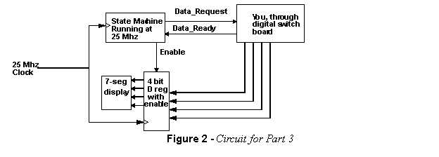
3 To transmit data between two devices, it
is often necessary to provide what are called “handshaking”
signals that ensure that the data is received correctly, particularly when two devices are running at very different
speeds. Consider the situation illustrated in Figure
1, in which
n bits of data are to be
transmitted from Device #2 to Device #1. When Device #1 requires new data, it
raises the Data_Request line high (to “1”). Once Device
#2 sees this and has placed the correct data on the n Data
lines, it raises the Data_Ready line high. When #1 has
taken the data (typically by storing it in a D- register) it lowers the Data_Request line after which #2 lowers the Data_Ready
line. Device #1 can only raise a new request after the Data_Ready line is lowered. This procedure is called a “full
handshake” and ensures that the data is transferred correctly, even when the
two devices are running at vastly different speeds.
An extreme example of two “devices” running at
different speeds is when you are one of the devices, and the other
device is a state machine clocked at 25MHz!
You are to build the circuit illustrated in
Figure 2 which uses the above protocol to simply transfer a 4-bit binary
number from you (using the digital switch board) into a 4-bit D register with
an enable signal. The state machine and D register must
be clocked at 25Mhz, and you must fully implement the protocol described above.
The state machine should continuously request data from you, which you will
provide through the data switches. When you indicate that the data is ready (by
raising the data_ready signal), the state machine should enable the D-register
for one clock cycle only, thus acquiring the data in the register. Connect your
7-segment circuit from lab #3 to the output of the D register so that you can
always see what is in the D-register. Your state machine must not request a new
data item until the Data-Ready line is lowered.
Build your state machine using VERILOG, but
construct your D-register using the graphic editor, and connect the state
machine to the register using the graphic editor.
1.
Implement and test the circuit of part
1 of the preparation.
2.
Implement and test the circuit of part
2 of the preparation.
3.
Implement and test the circuit of part
3 of the preparation. If you encounter difficulty (and perhaps even if you
don’t), make use of the logic analyzer to see what is happening in this
high-speed circuit.