|
|
| This page contains basic information describing the use of the VGA output port provided on the Altera UP1 Educational board. VHDL source code for a simple VGA controller ( VgaCon ) is provided. The purpose of VgaCon is to isolate the details of VGA signal generation from all the other modules in a design. VgaCon allows the pixel information to be written into its video memory using a very simple interface, while it is alone responsible for generating the required signals for displaying the pixel information on a VGA monitor. Thus for modules interfacing with VgaCon, the process of drawing on the screen consists of a request to colour a point located at any valid row and column. |
![]() A
simplified model of the VGA monitor and Controller.
A
simplified model of the VGA monitor and Controller.
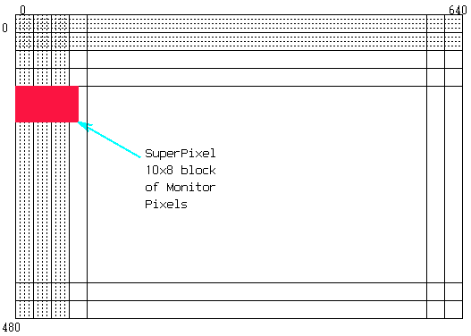 The VGA monitor can be thought of as a grid of pixels (picture elements which can be individually set to a specific colour). It contains 480 rows of 640 horizontal pixels. Most monitors, including VGA, use a serial scheme to set the colour of each pixel. This means that the VGA controller sends the colour information for each pixel one at a time, rather than being able to set all of the colours at once in a parallel scheme. This colour information for each pixel is provided by a RGB (Red, Green, Blue) triplet. Three analog signals are used represent relative amounts of red, green and blue that compose the colour. However, the UP1 board produces digital signals. Thus the controller will only be able to provide full intensity or turn off each of the RGB components. The protocol for the transmission is shown below. 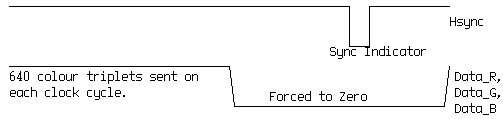 The Horizontal Cycle is part of the VGA standard defines a method for setting the colours of all the pixels in a particular row. The colour values for the 640 pixels are sent out on each of the first 640 clock cyles. The colour values are then forced to zero (black), while the Hsync signal is asserted low to provide synchronization for the monitor. The exact timing between these signals is defined in the VHDL source code for the VGA controller. 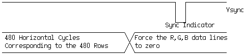 The Vertical Cycle allows the monitor synchronize which rows are being written by the Horizontal Cycles. 480 Horizontal Cycles are produced during the first stage of the Vertical Cycle. In the next stage, the colour values are again forced to zero (black), while the Vsync signal is asserted. The Vsync signal syncs the data following with the first row by telling the monitor to go back to the (0,0) pixel. |
|
| NOTES:
It is important to note that the monitor does not save any of the colour information written to it. The colour information must be stored in memory and continuously written to the monitor for the image to remain stable. VgaCon contains contains some memory where it stores the location and colour infomation that is supposed to be drawn on the screen. However, the FLEX10K70 does not have enough on-chip memory to save a value for each monitor pixel. A simple solution to the problem of not having enough memory is to map a large block of monitor pixels to a single memory location. In the Monitor diagram above, a 10x8 pixel block ( called a SuperPixel ) is mapped into a single location in memory. This scheme produces a virtual resolution of 64x60 SuperPixels. VgaCon actually stores a grid of 64x64 SuperPixels in its memory. However the last four rows are not displayed. |
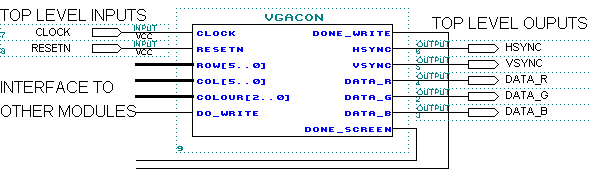
![]() VgaCon
Port Functionality.
VgaCon
Port Functionality.
 |
||
| Port/
Param |
Description | |
| Ramfile | This is a parameter which should be assigned to the MIF file which will contain the initial contents of the controller RAM memory. It allows one to easily create an initial picture that is displayed on the screen. A utility is provided below which can convert standard graphic files to MIF format. | |
| Clock | This port should be connected to the clock pin in the top-level design. The VGA controller requires that the clock pin is connected to the onboard clock on the UP1 board for correct functionality. This can be accomplished by assigning the clock pin to pin 91 on the FLEX10K70. | |
| Resetn | The resetn port should connect to an active low signal which forces the controller back to its initial state. Typically this port should be connected to the resetn pin in the top-level design. | |
| Done_Screen | This signal indicates that the entire screen has been drawn. The controller asserts this signal high for one cycle every 16.6ms. This signal is useful for timing and delay purposes. The Demo program uses this signal to flash a diagonal line on the screen approximately every half-second. | |
| Hsync | Produces the Horizontal and Vertical sync signals. These ports must connect to top-level output pins that must be assigned to pins 240 and 239 respectively on the FLEX10K70. | |
| Vsync | ||
| Data_r | Produces the red, green and blue signals corresponding to the contents of the VGA controller RAM. Again, these ports must connect to top-level output pins which are assigned to pins 236, 237 and 238 respectively on the FLEX10K70. | |
| Data_g | ||
| Data_b | ||
| Row[5..0] | These ports should each be connected to a 6-bit signal. The signals define the row and column coordinates of the SuperPixel that you wish to be placed on the screen. These coordinates are automatically transformed into an address for the controller in memory. As noted above the column number should be between 0..63, while the row number should be between 0..59 for the SuperPixel to be displayed on the monitor. | |
| Col[5..0] | ||
| Colour[2..0] | This port should be connected to a 3-bit signal which defines the colour of the SuperPixel to be placed on the screen. *Although eight possible colours can be produced by the digital RGB signals, three bits per colour would consume a lot of the dedicated memory blocks in the FLEX10K70. In order to allow more flexibility in your project, only two colours are supported so that less resources are consumed. | |
| Colour = "000" |
|
|
| Colour = "001" |
|
|
| Do_Write | This signal must be asserted high to write the SuperPixel defined by (Row[5..0], Col[5..0], Colour[2..0]) into the controller memory. However, because the controller is reading information from memory most of the time, the controller will wait until it is not reading from memory before it services the write. When the controller is reading from memory the done_write signal is '0' and you must wait until the done_write signal is '1'. When done_write is '1' the SuperPixel is written on the next positive clock edge. At that point you can lower do_write or keep it high to write a new SuperPixel on the next clock cycle. You can write a new pixel on every clock cycle until done_write is '0'. | |
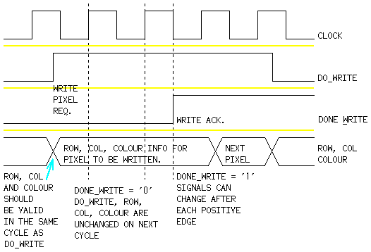
| Done_Write | This signal is '1' when the controller is not reading from memory. It indicates that if do_write is '1' a SuperPixel will be written on the next positive clock edge. You can write a new pixel every clock cycle for as long as done_write stays high. When done_write is '0' the controller is reading from memory and you must wait until done_write is '1' for your write to complete. A graphical depiction of the relative timing is shown in the diagram below. With a 25 MHz clock, it will take between 25 and 30 microseconds until done_write is '1' for the first time. When done_write returns to '0' it will take a similar amount of time for it to be '1' again. So when simulating with a 25 MHz clock, be sure to set the simulation end time to at least 30 microseconds to see done_write change. | |
 |
||
![]() Files
for Download.
Files
for Download.
| File | Description |
| VgaCon.vhd
(HTML) |
Simple VGA controller written in VHDL. |
| Demo.v | A Verilog file which demonstrates the use of VgaCon. When compiled and downloaded into the FLEX10K70 on the UP1 board, it will immediately display a picture of a mailbox and show a blinking diagonal line. More info provided in the source code. |
| Demo.csf | Contains the PIN and DEVICE assignments for the VGA Demo. Place this file in the same directory as the project file and the pins will automatically be assigned correctly. |
| Demo.quartus | The Quartus II project file for the VGA Demo. |
| Demo.mif | Initial RAM contents for the VGA controller. This contains the picture of the mailbox that is displayed initially by the Demo. |
| PBMtoMIF.c | Converts a graphics file in PBM(ASCII) format to a MIF file that can be loaded into the VGA controller RAM memory. This program was used to convert a PBM graphic of the mailbox into the Demo MIF file. It is particularly useful if you wish to create an initial background for applications such as tic-tac-toe game. You can draw the background with any graphic editor, shrink it to a 64x64 resolution and save it in PBM format. xv is an X Window program that will allow one to convert common graphic formats such as GIF, JPEG, and BMP to PBM. |
|
|
|
ECE 241 HOME PAGE | Send Comments/Suggestions/Complaints about VgaCon
Created by Deshanand
Singh
Modified by Aaron
Egier
Last Modified Nov 25, 2003.