ECE241F - Digital Systems - Lab 7
Complex Finite State Machine, Modules and Handshaking
Fall 2005 S.
Brown, J. Rose, K. Truong, B. Wang
1.0 Purpose
The purpose of this lab is to gain
experience with state machines by building a much larger one that controls a
small adder/subtracter unit. This lab amounts to building a very simple
processor (computer). The lab also teaches about using pre-designed functional
units and uses the handshaking technique explored in Lab #6 to
properly synchronize communication between two devices running at different
speeds.
Warning: this lab is difficult - be sure to allocate
sufficient time for preparation. The good news is that you will learn a great
deal in this lab.
2.0 Background
1.
In Lab #5 you created a 3-bit D-type register (which was simply three D
Flip-flops with the clock signals connected together), that also had a reset
signal which set all of the flip-flops to zero when activated. From Lab #6 you
will recall that a register with an Enable signal works
in the following way: if the Enable = 1, then the register works as usual in
response to the clock. If Enable = 0, then the outputs (Qi)
do not change in response to the clock.
2.
The Altera Quartus software provides you with a number of pre-designed
units, called the Library of Parameterized Modules (LPM), one of which you have used already
to create a 3-bit D register. More generally these consist of
adders, adder/subtracters, multipliers, shift registers, decoders and more -
basically everything you’ve been designing in this course, already done for
you! The meaning of the word “parameterized” here is that you can specify many
different things about the module. For example, you can create an adder and
specify that it should be a 10 bit adder, or a 20-bit adder. You can specify
that a multi-bit D register has an enable signal (or not).
To look at the different modules that are available, bring up
the schematic editor in Quartus and double-click to bring up the Symbol dialog box. Double-click on the c:/altera/quartus50/libraries,
then megafunctions then arithmetic. The list of symbols that
appear are the many different pre-designed modules that are available. Scroll
down the list and select the module lpm_add_sub. This
is a module that will act either as an adder or a subtracter, depending on an
input control signal.
When you select the lpm_add_sub, a symbol appears on the graphic
editor and at the same time a dialog box (a "wizard") appears. This
dialog box allows you to provide specifications of the type of adder/subtracter
that you require. (It first asks you which language you'd like the symbol to be
written in, so choose Verilog). The next page of the wizards asks "How
wide should the 'data' and 'datab' input buses be?" Dataa and Datab refer
to the input wires of the adder/subtracter, so to obtain a 3-bit adder/
subtracter, set this number to 3.
To specify that you want this to be an adder/subtracter unit (as
opposed to simply an adder), on the same page, click the button that says:
"Create an 'add_sub' input port to allow me to do both (1 add; 0
subtracts)." This creates a signal, attached to the adder, called add_sub, which when set to 1, causes the device to add its
two inputs, and when set to 0, makes it subtract them. (Later in class, we will
show a circuit that does this). Make sure that it has the correct “currently
selected device family” as MAX 7000S. The wizard will ask you several other
questions, suggesting other features of the adder which you won't need. Once
you "Finish" with the wizard, you'll be able to place the symbol for
the adder-subtracter like any other schematic symbol. You can modify any
choices you made during the wizard by double-clicking on the result symbol and
walking through the editor again.
To learn more about the various parameters of this module, you
can read the "help" documentation by selecting Help from the top menu
and searching for lpm_add_sub.
2.
Recall from lab #6, that to transmit data between two devices, it is
often necessary to provide handshaking signals that ensure that the data
is transmitted and received correctly. This is particularly true when two
devices are running at very different speeds. Consider the situation
illustrated in Figure 1, in which
n bits of data are to be
transmitted from Device #2 to Device #1. When Device #1 requires new data, it
raises the Data_Request line high (to “1”). Once #2
sees this and has placed the correct data on the n Data
lines, it raises the Data_Ready line high. When #1 has
taken the data (typically stored in a D-register) it lowers the Data_Request line after which #2 lowers the Data_Ready
line. Device #1 can only raise a new request after the Data_Ready line is lowered. This procedure is called a “full
handshake” and ensures that the data is transferred correctly, even when the
two devices are running at vastly different speeds.
We will make use of this concept in this lab, because Device #1
will be a state machine running at 25 MHz, and device #2, will be you, (i.e. you will be providing both the data through
switches, and the Data_Ready signal) and you run considerably slower than
25MHz. This is very similar to the machine you built in Lab #6.
3.0 Preparation
Note: all preparation schematics,
VERILOG code and simulation output MUST BE PRINTED on
paper and pasted into your lab book for marking, before the lab begins.
1.
Using the schematic editor, create a 3-bit D-type register symbol that
has a synchronous Reset
signal and an Enable signal as described above (either
by creating your own symbol from basic DFFs or by using module lpm_DFF found
under the megafunctions library in the storage folder). You
should be familiar with the enable function of this register from Lab #6.
2.
Create a 3-bit adder/subtracter LPM unit in the schematic editor, (with
an add_sub control signal) as described in part 2 of the background. Simulate
the unit to make sure that you understand how it works. It is easier to
simulate if you keep the 3- bit inputs grouped as a bus, and in the waveform
editor, specify these as a group.
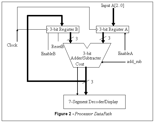
3.
Build the circuit of Figure 2 below in the graphic editor.
Simulate this circuit to add two numbers, applied one at a time through the
input A, similar to Lab #5.
4.
Using the circuit of Figure 2, simulate the subtraction of two
numbers. (Setting add_sub = 0 makes this unit a subtracter).
5. You are to design a finite state machine that controls
the circuit of Figure 2, and interacts with you as the user. The clock
signal (for both the finite state machine and the Registers A and B)
will be connected to the 25MHz (period 40ns) clock signal that is generated on
the Altera board, and appears at pin #83 of the MAX 7128 (the global clock
input).
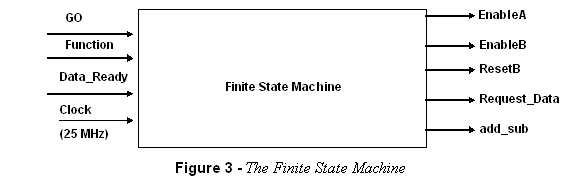
The outputs of the finite state machine (illustrated in
Figure 3 ) are:
i.
EnableA - the enable signal for register A. When this is turned on,
register A will, on the next positive edge of the clock, copy the input data
A[2..0], coming from user switches into register A.
ii.
EnableB - the enable signal for register B. When this is turned on,
register B will, on the next positive edge of the clock, copy the output of the
adder/ subtracter into register B.
iii.
ResetB - an active-low signal which should set the contents of register
B to zero. Make this a synchronous reset.
iv.
Request_Data - is an output (to be hooked up to a light on the digital
switch board) which will signal to you that the machine wants you to input
data.
v.
add_sub - is connected to the add_sub signal of the adder/subtracter, to
tell it which function to perform. (=1 means add, =0 means subtract)
The inputs of the finite state machine are:
i.
GO - active low (i.e. active when signal = 0). When activated, this
causes the machine to begin operation, as described below.
ii.
Function - this is an input from the user which indicates the
“instruction” that is desired. Function = 1 means that the two numbers should
be added. Function =0 means that the two numbers should be subtracted.
iii.
Data_Ready - this signal should be connected to a switch on the switch
board. It is the other part (with Request_Data) of the handshake between you
and the state machine. Once the data is ready, you raise the Data_Ready signal.
Once the Request_Data signal is lowered, you must lower the Data_Ready signal.
When the GO signal is activated, your machine should request two
pieces of 3-bit data from the user (one at a time) and either add or subtract
them, depending on the Function input. To obtain the
two pieces of data, you must use the handshaking protocol described above in
the background section. Code your Finite state machine in Verliog.
Turn it into a symbol and connect it to the circuit of Figure 2 using the
schematic editor.
4.0 In the Lab
Build and test the circuit of part
5 of the preparation. Make sure that all of the clock signals on flip
flops and the state machine are connected to the 25MHz clock (pin 83 of the
7128). Use the logic analyzer to show the operation of the circuit.