ECE241F - Digital Systems - Lab 2
Introduction to Programmable Logic using FPGAs, Quartus II CAD Software Tutorial and Using the Logic Analyzer
1.0 Purpose
The purpose of this lab is to learn the basics of the Altera Quartus II CAD (Computer Aided Design) software that you will use throughout the course. You will learn to design using both schematic entry and hardware description language, called Verilog. You’ll learn to simulate your circuit on a computer to determine if it is correct, and how to tell your computer to “synthesize” your circuit into a form that can be loaded into a Field-Programmable Gate Array (FPGA). Lastly, you will use the basic weapon of all digital design debugging: the Logic Analyzer.
Warning: there are many new concepts and things to do in this lab! Don’t worry if it doesn’t make sense the first time around; you’ll be surpised about how naturally it will all come to you by the end of the course.
2.0 Preparation

- The first task is to become familiar with the Altera Quartus II Version 6.0 CAD software. A CD-ROM containing the software has already been distributed in your ECE241 lecture. Alternatively, you can download a copy of the software online as described in the handout titled “Access to CAD Software.” The online and CD-ROM version are identical, so you don’t have to worry if you didn’t receive a copy of the CD.
i. Read and do Sections 1 to 6 from the “Quartus II Introduction Using Schematic Design” that is located at http://www.eecg.toronto.edu/~jayar/ece241_06F/tut_quartus_intro_schem.pdf.
ii. Read and do Sections 1 to 6 from the “Quartus II Introduction Using Verilog Design” that is located at http://www.eecg.toronto.edu/~jayar/ece241_06F/tut_quartus_intro_verilog.pdf. You will find a lot of the information is the same as that found in the first tutorial, and so feel free to skim over the familiar content.
iii. Read and be prepared to do Section 7.0 and 7.1 from the “Quartus II Introduction Using Verilog Design” to learn how to program the DE2 Educational Board during the lab.
- Design, enter and simulate a circuit, using both schematic entry and Verilog as the design entry method (i.e. do it twice, with the two methods), that implements the two logic functions, f1 and f2, with four inputs named a, b, c and d.
i. The function f1 should be 1 when either a = c or b = d, but not when both a = c and b = d.
ii. The function f2 should be 1 when the number of 1’s in a, b, c and d is even. (That is, count the number of 1’s in the four variables; if the count is even, then f2 is 1, otherwise it is 0.)
Give the truth tables for functions f1 and f2. Then derive a Boolean expression in canonical sum-of-products (canonical sum-of-products means sum of min-terms only) form for each function. Use algebraic manipulation to simplify the expressions. Enter the simplified Boolean expressions into Quartus II in two different ways:
i. Draw a schematic that includes the logic gates for both f1 and f2.
ii. Write Verilog code that represents both f1 and f2 with Boolean equations.
- You must either place all your design files on your home directory on the ECE ugsparcs computers, or bring a USB Storage Key containing your files. Instructions for using the ugsparc computers are provided in Section 4, below.
3.0 In the Lab
- Begin with Section 6, and follow the instructions there.
- Download and test the circuit of from Part i of Question 1 in the preparation. Demonstrate your circuit to a TA.
IMPORTANT: While switches and lights exist on the Altera DE2 board, we require that you use the digital switchboard instead. To use the digital switchboard your lab setup will have to appear as illustrated in Figure 1. On the left hand side there is the digital switchboard, a switchboard-to-DE2 adapter is in the middle, and the Altera DE2 board is on the right hand side. The digital switchboard is connected to the header labelled “PIT” on the adapter using a 40-pin ribbon cable. To complete the connection, the header labelled “DE2” is connected to the Altera DE2 board using another 40-pin ribbon cable. The 40-pin ribbon cable should be attached to the JP2 header on the Altera DE2 board (see Figure 2).
With the setup described above the general
purpose IO header JP2 can be used to receive input from (and produce output to)
the digital switchboard. The following 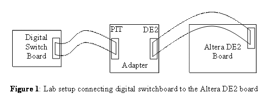 table shows the digital switchboard function, the
pin on the JP2 header it is found on, and the pin assignment you need to
make in Quartus II to use the function.
table shows the digital switchboard function, the
pin on the JP2 header it is found on, and the pin assignment you need to
make in Quartus II to use the function.
|
Digital Switchboard Function |
JP2 Header Pin Number |
Altera Cyclone II Pin on the DE2 Board |
|
Switch #1 |
1 |
PIN_K25 |
|
Switch #2 |
3 |
PIN_M22 |
|
Switch #3 |
5 |
PIN_M19 |
|
Switch #4 |
7 |
PIN_N20 |
|
Switch #5 |
9 |
PIN_M24 |
|
Switch #6 |
13 |
PIN_N24 |
|
Switch #7 |
15 |
PIN_R25 |
|
Switch #8 |
17 |
PIN_R20 |
|
Light #1 |
2 |
PIN_K26 |
|
Light #2 |
4 |
PIN_M23 |
|
Light #3 |
6 |
PIN_M20 |
|
Light #4 |
8 |
PIN_M21 |
|
Light #5 |
10 |
PIN_M25 |
|
Light #6 |
14 |
PIN_P24 |
|
Light #7 |
16 |
PIN_R24 |
|
Light #8 |
18 |
PIN_T22 |
|
Pulse |
37 |
PIN_V24 |
|
Clock |
39 |
PIN_W25 |
- Download and test your circuit from Part 2 of the preparation, and show it to a TA.
- Perform the exercises outlined in Section 5 using the Logic Analyzer.
4.0 ECE Solaris-Based “ugsparc” Computer File Server
The ECE ugsparc machines are Solaris operating systems (as opposed to Windows or Linux) computers available to undergraduate 2nd year and over ECE students. Solaris is very similar to Linux. They are located in the south corridor of the Galbraith building, second floor, rooms GB 243 and GB 251. Their main use, for the purposes of this course, is as a place to deposit your design files, from home through the internet.
The ECE upgsparc machines can be accessed remotely by connecting to either ugsparc251.eecg.utoronto.ca or ugsparc253.eecg.utoronto.ca using secure shell – which you will have used in APS105 in first year.
You can access these remotely from your home for general computing or file storage purposes. Your login name for the ECE ugsparcs is the same as your ECF account. The password is the same as your ECF password. If you don’t have either an ECF account or an ECE account, request one from ECF (in Engineering Annex 2nd floor) and then send a request to tim@eecg.utoronto.ca to create an ECE ugsparcs account.
5.0 Using the Logic Analyzer
A logic analyzer is the digital equivalent of the oscilloscope used in the analog world. It is used to observe the value of the digital signals present on wires over a period of time. The logic analyzer is essential for debugging any digital circuit. In this lab we will show you how to use the logic analyzer to observe time-varying digital signals.
More information on the operation of the two types of logic analyzers found in the labs can be found at:
http://www.eecg.utoronto.ca/~aulich/logicmix.html
and http://www.eecg.utoronto.ca/~aulich/logicmix2.html
During the lab, a Teaching Assistant will show you the basics of how to use the logic analyzer. Once this has been done, do the following:
1. Output the 50MHz clock (CLOCK_50) on the DE2 board to a GPIO pin (i.e. GPIO_0[0]) on JP1. The location of JP1 is shown in Figure 2. The pin assignments for the GPIO pins can be found in the repository for pin assignment files.
2. Connect the 50MHz clock to the input from one of the inputs from part 2 of the prepration. Use the logic analyzer to observe both outputs (f1 and f2) of that circuit.
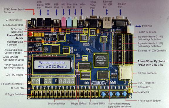
Figure 2 – DE2 Educational Board Overview
6.0 Using the PC and the DE2 Board in the Lab
This section tells you how to access the files you have placed on the ECE ugsparc machines from the PCs in the labs in Rooms Bahen 3135, 3145, 3155 and 3165.
1. Turn on the PC and monitor. The PC should be showing you a login prompt. If not, reboot it using the Start menu in the lower left hand corner, by selecting the “shutdown” menu item. Make sure that the “domain” you log into is selected as Gizmo. Your login name is the same as the ECF and ECE ugsparc login, and your initial password is your 9 digit student number (change this right away). Your ECE ugsparc home directory will be mapped to the W: drive. You should be able to see all of the files you have placed there.
2. Connect the power supply to the DE2 Educational Board.
3. Connect the DE2 Educationl Board to the PC using a USB cable.
4. To connect the DE2 Educational Board to the Digital Switch Board that you used in Lab #1 there will be an adaptor board provided along with the DE2 board.. Connect a 40-pin cable from JP2 on the DE2 Educational Board (shown on the right hand side of Figure 2, near the top) to the adapter using a 40-pin cable. Connect the other port on the adapter to the Digital Switch Board using another 40-pin cable.
5. Turn on the station power supply.
6. Turn on the DE2 Educational Board.
7. Start the Quartus II program by opening the “Courseware” directory and double-clicking on the Quartus II icon. It should take less than a minute to load.
8. With Quartus II running, you can open your project and compile your design as described in the Tutorials. Make sure that you have correctly connected the pins in your design.
9. Download and test your circuits using the instructions provided in the Tutorials, as indicated in Section 3.0.