ECE241F - Digital Systems - Lab 3
More Complex Logic Design:
7-Segment Displays and Hierarchical Design
1.0 Purpose
The purpose of this lab is to build several more complex logic circuits and to gain increased familiarity with the Quartus CAD software. It is also to learn how to create more complex circuits using a hierarchical design approach – groups of groups of circuits.
2.0 Background
- A seven-segment display is often used on computers, watches, DVD players and many electronic devices to display numbers and some characters. It consists of seven independent lights, actually light-emitting diodes (LEDs), in an “8” configuration as shown below in Figure 2. By turning on different segments, you can display different numbers and some letters.
- Read section B.5 (labelled “Mixing Design-Entry Methods”) from “Appendix B, Tutorial 1 – Using Quartus II CAD Software” that is located at http://www.eecg.utoronto.ca/~jayar/ece241_06F/textb.pdf.
3.0 Preparation
You are to create two logic circuits to drive one of the seven-segment displays on the Altera programmable logic board. Please see Section 5.0 for details of how to use the 7-segment display on the DE2 Educational board. (In particular, note that to turn a light-segment on, you must drive the corresponding pin to a logical “0”).
1. Design a circuit that takes a four bit (X3, X2, X1, X0) input from the digital switch board, and drives the 7 segment display HEX0 on the DE2 board as described in the table below. Note that for the letters, some are capitalized and some are not. (The reason is that a capital B, for example, would come out the same as an 8 on a 7- segment display, so we will display a lower-case b instead).
|
X3 X2 X1X0 |
Display (note the capitalization) |
|
0000 |
0 |
|
0001 |
1 |
|
0010 |
2 |
|
0011 |
3 |
|
0100 |
4 |
|
0101 |
5 |
|
0110 |
6 |
|
0111 |
7 |
|
1000 |
8 |
|
1001 |
9 |
|
1010 |
A |
|
1011 |
b |
|
1100 |
C |
|
1101 |
d |
|
1110 |
E |
|
1111 |
F |
Table 1
Determine the equations for the 7-segment display segments, and minimize them using the Karnaugh-map method described in class. Write Verilog code to represent the logic function for each segment as a Boolean equation (using just the AND (&), OR (|), NOT (~) operators). Simulate and test your equations using the Quartus functional simulator, or with the timing simulator with the Cyclone II device set.
- Convert the 7-segment decoder circuit you have created in the previous step into a symbol as you have learned from part 2 of the preparation (using File à Create/Update à Create Symbol Files for Current File). You will be extensively using the 7-segment decoder symbol that you have created in following labs. It is most important to realize that from now on, when you want to use the 7-segment decoder, you need not concern yourself with the inner-workings but simply feed it the higher-level 4-bit input and connect it to the desired HEX display on the DE2 Educational board.
- Design a similar circuit to the one given in part 1,
except that you should use the four input switches to generate the letters
of your last name. For example, if your last name is Parnas, you could use
code 0000 to display a P, 0001 to display an A, 0010 to display an R (or
something as close to an R as you can get). Note that you can choose any
code you wish for each letter. Notice also that you don’t need to create
two codes for a letter that appears twice in your name. For example, the
letter A appears twice in Parnas, but you only need to produce one code
for the letter A - the intent is that you will be able to spell out your
last name on the 7-segment display by entering the codes for the letters
one at a time.
For Fairness: if your last name is longer than 9 unique letters, you need only do 9 unique characters of it. If your last name is shorter than 9 characters, you must add more letters from your first name until you have coded at least 9 unique characters.
Since you will only need to do 9 codes, you should make use of the don’t cares that will be available in the truth tables.
4.0 In the Lab
1. Power up the DE2 Educational Board to verify that the 7-segment displays are functioning properly.
2. Download and test the circuit from Part 1 and Part 3 of the preparation. Show each working circuit to the TA.
5.0 Hex (7 Segment) Displays on the DE2 Board
The DE2 Educational Board has 8 Hex (7-segment) displays. These displays, as with almost everything on the DE2, are connected directly to the pins of the chip. The figure below shows the indexing of each segment.
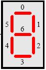
Figure 2
The table below shows how the segments in Figure 2 correspond to the pin names from the DE2_pin_assignments.csv file.
|
Display Segment |
Wires for HEX0 |
Wires for HEX1 |
|
0 |
HEX0[0] |
HEX1[0] |
|
1 |
HEX0[1] |
HEX1[1] |
|
2 |
HEX0[2] |
HEX1[2] |
|
3 |
HEX0[3] |
HEX1[3] |
|
4 |
HEX0[4] |
HEX1[4] |
|
5 |
HEX0[5] |
HEX1[5] |
|
6 |
HEX0[6] |
HEX1[6] |
The same naming convention is used for all of the Hex displays on the DE2 board.