ECE241F - Digital Systems - Lab #4
Sequential Logic
1.0 Purpose
The purpose of this lab is to learn about the basic operation of sequential logic (circuits with memory), by building them up from basic gates. You will also build a shift register from flip flops, and learn how to invoke flip-flops in the Verilog language. As a side-effect, you will also be reviewing the hierarchical concepts encountered in the previous lab.
2.0 Background
1. In class you have learned about the basic circuit for RS latches, D latches, clocked D latches and master-slave edge-triggered D flip-flops, so you should review your notes on these.
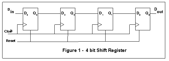
2. A shift register is typically used to send and receive data, one bit at a time, under the control of a clock signal. Figure 1 below illustrates a 4-bit shift register built using positive-edge triggered D-type flip flops. On each positive clock edge, the value of the signal Di is copied onto the value of Qi. It takes four clock cycles for the original value of Din to appear at Dout. The entire contents of the shift register can be initialized by resetting each flip-flop with a reset signal.
3. Recall that, in Lab #3, you created a 7-segment segment decoder and converted it into a symbol so that it can drive any of the 7-segment displays on the DE2 Educational Board using any desired input. We’ll be using that design in this lab as well.
3.0 Preparation
Design and simulate (using timing simulation) the following circuits, using the graphic schematic editor of Quartus (DO NOT USE Verilog, except for part 5). You should design all of these circuits with gates from the basic logic primitives library. Make a separate directory for each of the circuits you design. Parts 1, 2, and 3 concern the basic operation of circuits that have memory, and so you are required to design these from basic logic gates such as NAND and NOR.
- A set-reset latch, using cross-coupled 2-input NOR gates.
- A level-sensitive clocked D latch, based on the set-reset latch you designed in #1.
- Turn the D-latch into a symbol, as you did in Lab 2, and use it to design a negative edge-triggered master-slave D flip-flop. Remember that you should do this by creating a separate project for the D-type Master Slave Flip-flop.
- Building a shift register to serially drive a 7-segment display:
i. Create a four-bit shift register (as illustrated above in Figure 1) from D flip-flops, and turn it into a symbol as you did for the D-latch in part 3. Instead of using the flip-flop you designed in part 3, use the D flip-flops available in the “primitives” library, “storage” subsection (as the symbol “DFF”). Make sure that the four outputs Q3, Q2, Q1, and Q0, are available as outputs from your shift register. Note that there are D flip-flops inside the Logic Elements (LEs) of the Cyclone II FPGA, and so you actually don’t need to build them using combinational logic.
ii. Design, enter and simulate a circuit that connects the outputs of the shift register (Q3Q2Q1Q0) to the inputs X3X2X1X0 of your circuit from Part 2 of Lab #3. The inputs to your circuit should be a single Din signal and the clock. The point here is to generate the inputs to your circuit from Lab #3, serially, one bit at a time, rather than in parallel, four bits at a time.
- The following exercises should be completed using the Verilog language as the method of circuit entry:
i. Build and simulate an edge-triggered D-type flip flop as described in the text Section 7.12.2 on page 388 of the text. (It is probably best to read from Section 7.12.2 through Section 7.12.5)
ii. Build and simulate a 3-bit D register the same way, with an asynchronous reset signal as described in Section 7.12.5. Do not confuse the D register with a shift register. The D register shifts data in parallel sense and not serially.
- Building a waveform generator.
i. Build a 10-bit shift register in the manner that was described in part 4 above, including the “reset” signal. Connect the output of the final bit’s Q output to the first bit input of the D register (the Din of the shift register) so that the shift register actually forms a ring. Notice that a DFF has both a “Reset” input (labelled CLRN) and “Preset” input (labelling PRN), which are active low. CLRN sets the bit to be a low, and PRN sets it to be a high value, asynchronously to the clock. Connect your reset signal to some of the flip flop’s CLRN inputs, and connect some to the PRN input (you choose which).
ii. Simulate the circuit by activating the reset for an appropriate period, which effectively loads a value into the shift register. Continuous clocking of this circuit produces a waveform of your design, based on which flip-flops you reset or preset. In the lab you will connect the clock of the flip flops to the on-board system clock that runs at 50MHz. When you operate the circuit, activate the reset, and then observe the output of the shift register using the logic analyzer.
- Optional: Building a ticker to scroll your birth date:
i. Recall that to drive a 7-segment display, we need a four bit-input. Create a new design and build four 4-bit shift registers in the same manner that was described in part 4 above, including the “reset” signal. The clock of the shift register, as above, will be a switch.
ii. For each 4-bit shift register, connect the output of the last DFF to the input of the first DFF (i.e. Q0 à D3), so that each shift register forms a ring. This will allow our ticker to rotate.
iii. In your design, create four 7-segment decoders and connect them to four of the 7-segment (HEX) displays on the DE2 board. Use the first bit (i.e. Q3) from each shift register to drive the first HEX display, the second bit (i.e. Q2) to drive the second HEX display, and so on. Take note that we made 4 shift register rings because our 7-segment decoder has 4 inputs.
iv. Notice that a DFF has both a “Reset” input (labelled CLRN) and “Preset” input (labelling PRN), which are active low. CLRN sets the bit to be a low, and PRN sets it to be a high value, asynchronously to the clock. You will encode your birth date in a MMDD format by connecting your reset signal to some of the flip flop’s CLRN inputs, and some to the PRN input. For example, if you birth date is March 23rd, it is encoded as 0323. So the first DFF from each shift-register should be set up to encode 0, the second should encode 3, and so on. In your simulation, activate the reset for an appropriate period, which effectively loads the preset values into the shift registers.
4.0 In the Lab
Implement and test all of the circuits you designed in the preparation. Show each working part to a Teaching Assistant. (Note, as there are many parts, you may wish to show several working parts at once to a TA).
If you choose to build the optional circuit in part 7, output the clock, the output from one of the flip-flops, and ground onto three of the GPIO pins on JP1. Connect these pins to the logic analyzer, connecting the outputted ground to the logic analyzer ground, and observe the outputs.