ECE241F - Digital Systems - Lab 5
Adders and Registers
1.0 Purpose
The purpose of this lab is to introduce the logic needed to create an adder, and use it in combination with registers. You will describe the circuit using both schematic entry and Verilog. This lab also introduces and constructs a circuit that you will use in the lab #6 in a more sophisticated way.
2.0 Background
- In Lab #3, you created a 7-segment display decoder, which you also used in Lab #4. You will be using it again to show the output of an adder.
- In Lab #4, you created a 3-bit D register that used an asynchronous reset, which changes a register’s output as soon as the reset signal activates, regardless of the clock. In this lab you will use a synchronous reset of a D register which means that the reset doesn’t occur until the next active clock edge.
- In this lab, you will create an adder and use it in conjunction with D registers and the 7-segment display to create the simple arithmetic unit as shown below in Figure 1. Its inputs are: a single three-bit binary number (X2X1X0), the Clock, and the Reset signal. In the preparation below, you are required to figure out how to use this circuit to add two 3- bit numbers. This is actually a simple version of the arithmetic and logic unit that can be found inside all computers.
- The Altera Quartus software provides you with a number of pre-designed units, called the Library of Parameterized Modules (LPM). These consist of adders, adder/subtracters, multipliers, shift registers, decoders and more - basically everything you’ve been designing in this course, already done for you! The meaning of the word “parameterized” here is that you can specify many different things about the module. For example, you can create an adder and specify that it should be a 10 bit adder, or a 20-bit adder. You can specify that a multi-bit D register has an enable signal (or not).
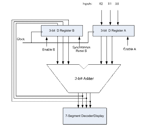
Figure 1 – Circuit to Be Designed in Section 3.0, Part 3 and 4
3.0 Preparation
- Determine the sequence of control signals and data inputs that you would need to be able to add two 3-bit numbers using the circuit of Figure 1. You will need to know this in order to properly simulate the circuit that you will design. The sequence is essentially a timing diagram (giving the sequence of the input values X2X1X0, Reset and clock) such as you would create using the waveform editor of Quartus to test the circuit. Give the timing diagram for this part of the preparation.
- Design a 3-bit ripple-carry adder, using the method of hierarchical schematic entry with the graphic design editor in Quartus. (i.e. build a single full adder from gates, and then use three of these, as symbols, to build the 3-bit adder). You should design the adder as a basic logic function – DO NOT USE the built-in LPM adder (lpm_add or lpm_add_sub). Simulate the adder using Quartus timing simulation to be sure that it works. Note that a 3-bit adder has two 3- bit inputs and one four-bit output. Convert your 3-bit adder into a symbol.
- Using the adder, two 3-bit D-type registers with synchronous reset, and your seven-segment decoder circuit from Lab 3, build the circuit of Figure 1 using the graphic editor. Simulate your circuit to ensure that it works. You can create a 3-bit D-register by using the Library of Parameterized Modules (LPM). In the schematic editor, double-click to bring up the Symbol dialog box. Double-click on the c:/altera/quartus60/libraries, then megafunctions then storage and select lpm_dff. To customize this “megafunction” use the wizard that pops up to get the right number of bits and the synchronous reset (clear). See the section titled “Connecting Buses in the Schematic Editor” below on how to connect the thick multi-wire “bus” that you will see when you place the lpm_dff on to your schematic.
- Design and simulate the same circuit using VERILOG only (i.e. do not use the graphic editor). You will need to read the VERILOG reference manual in Appendix A, and the descriptions in chapter 7 of your textbook closely in order to do this.
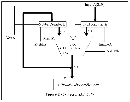
- Next we will design a circuit similar to the ones you have constructed in parts 3 and 4, except this time we will be using the the lpm_add_sub megafunction available to you in Quartus’ schematic editor. The circuit you are to construct is shown above in Figure 2. Follow the instructions below, which describe important parts on how to do this.
i. Using the schematic editor, add an lpm_add_sub module from megafunctions à arithmetic and simulate the unit to make sure that you understand how it works. It will be easier to simulate if you keep the 3- bit inputs grouped as a bus, and in the waveform editor, specify these as a group. This is a module that will act either as an adder or a subtracter, depending on an input control signal. When you select the lpm_add_sub, a symbol appears on the graphic editor and at the same time a dialog box (a "wizard") appears. This dialog box allows you to provide specifications of the type of adder/subtracter that you require. (It first asks you which language you'd like the symbol to be written in, so choose Verilog). The next page of the wizards asks "How wide should the 'data' and 'datab' input buses be?" Dataa and Datab refer to the input wires of the adder/subtracter, so to obtain a 3-bit adder/ subtracter, set this number to 3.
To specify that you want this to be an adder/subtracter unit (as opposed to simply an adder), on the same page, click the button that says: "Create an 'add_sub' input port to allow me to do both (1 add; 0 subtracts)." This creates a signal, attached to the adder, called add_sub, which when set to 1, causes the device to add its two inputs, and when set to 0, makes it subtract them. (Later in class, we will show a circuit that does this). Make sure that it has the correct “currently selected device family” as Cyclone. The wizard will ask you several other questions, suggesting other features of the adder which you won't need. Once you "Finish" with the wizard, you'll be able to place the symbol for the adder-subtracter like any other schematic symbol. You can modify any choices you made during the wizard by double-clicking on the result symbol and walking through the editor again.
To learn more about the various parameters of this module, you can read the "help" documentation by selecting Help from the top menu and searching for lpm_add_sub.
ii. Build the circuit of Figure 1 in the schematic editor using the adder/subtracter from part 5i and D registers from part 3. Simulate this circuit to add two numbers, applied one at a time through the input A.
iii. Using the circuit of Figure 1, simulate the subtraction of two numbers. (Setting add_sub = 0 makes this unit a subtracter).
4.0 In the Lab
- Build and test the adder circuit from part 2 of the preparation.
- Build and test the circuit from part 3 of the preparation.
- Build and test the circuit from part 4 of the preparation.
- Build and test the circuit from part 5ii of the preparation.
5.0 Connecting Buses in the Schematic Editor
To connect to a bus (which is what the thick lines labelled data[2..0] for the lpm_dff are called) it is a little tricky. First, you should use the thick wiring tool (the 6th icon from the top of the left side of the schematic editor) to pull out a length of the wire. Then, you need to label that wire by right clicking on it and selecting "properties". This will bring up a window in which you type the name of the bus; which you should label with something like: busout[2..0]. Then, when you want to connect individual (single, non-bus) wires to this, you don't actually make them touch. For each individual wire you want to connect, you right click on an extended wire and label it with a name that says which wire of the bus you want. For example, to connect a single wire to the first wire on the bus above, you would give it the name busout[2]. To connect to the second wire, you'd connect it to busout[1] and then busout[0].