ECE241F - Digital Systems - Lab 6
Finite State Machines and Handshaking
1.0 Purpose
The purpose of this lab is to become familiar with the design of Finite State Machines (FSM). You will design these finite state machines in two ways: from “scratch” where you create the entire circuit schematic, and using the state machine description method in Verilog. The first design will be clocked manually using a an external switch as in previous labs. The next two designs will be clocked using the 50 MHz on-board clock of the DE2. The second design will implement the handshaking protocol described in class. The third method uses the handshaking method to control the adder circuit you designed in the last part of Lab 5. You will use the logic analyzer to observer the behavior of these circuits.
2.0 Background
- In class we have described a simple state machine to “recognize” when a serial stream of bits has the pattern “11.” This is a machine that has three inputs: (reset, clock, and x, the data input) and one output, Y, which is set to 1 on the cycle following the “11” pattern. Part 1 of the lab is based on this.
- In Lab #5, you created a circuit to add two numbers, in part 5. You will use this circuit, but it will be clocked at 50MHz. You will use the technique of handshaking, described in class, to synchronize your data input with the circuit running at that high speed.
3.0 Preparation
- You are to design a sequence recognizer, like the one described in class, but this one outputs a “1” when the bit sequence 101 has occurred. The output 1 should be in the cycle following the last 1 of the pattern 101. Here is an example input/output sequence:
|
Clock Period # |
1 |
2 |
3 |
4 |
5 |
6 |
7 |
8 |
9 |
10 |
11 |
12 |
13 |
14 |
15 |
|
Input (Before +ve Clock edge) |
0 |
1 |
1 |
0 |
1 |
1 |
1 |
0 |
1 |
0 |
0 |
1 |
0 |
1 |
0 |
|
Output (Before +ve Clock edge) |
0 |
0 |
0 |
0 |
0 |
1 |
0 |
0 |
0 |
1 |
0 |
0 |
0 |
0 |
1 |
For clarity, here is the timing diagram (assuming zero delay of flip-flops) of the clock, input and output for the first six clock cycles correspinding to the table above:

Design this circuit using the graphic editor and basic gates only. DO NOT use VERILOG. The purpose here is to be sure that you understand basic circuit of a state machine. Your preparation should consist of:
i. The state diagram (draw by hand).
ii. The state transition table, with encoding - use the 1-hot encoding method.
iii. Your schematic.
iv. The simulation output.
- To transmit data between two devices, it is often necessary to provide what are called “handshaking” signals that ensure that the data is received correctly, particularly when two devices are running at very different speeds. Consider the situation illustrated in Figure 1, in which n bits of data are to be transmitted from Device #2 to Device #1.
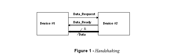
When Device #1 requires new data, it raises the Data_Request line high (to “1”). Once Device #2 sees this and has placed the correct data on the n Data lines, it raises the Data_Ready line high. When #1 has taken the data (typically by storing it in a D- register) it lowers the Data_Request line after which #2 lowers the Data_Ready line. Device #1 can only raise a new request after the Data_Ready line is lowered. This procedure is called a “full handshake” and ensures that the data is transferred correctly, even when the two devices are running at vastly different speeds.
An extreme example of two “devices” running at different speeds is when you are one of the devices, and the other device is a state machine clocked at 50MHz!
You are to build the circuit illustrated in Figure 2 which uses the above handshaking protocol to simply transfer a 4-bit binary number from you (using switches) into a 4-bit D register with an enable signal. The state machine and D register must be clocked at 50Mhz (the figure below says 25MHz in error), and you must fully implement the protocol described above. The state machine should continuously request data from you, which you will provide through the data switches. When you indicate that the data is ready (by raising the data_ready signal), the state machine should enable the D-register for one clock cycle only, thus acquiring the data in the register. Connect your 7-segment circuit from lab #3 to the output of the D register so that you can always see what is in the D-register. Your state machine must not request a new data item until the Data-Ready line is lowered.
|
|
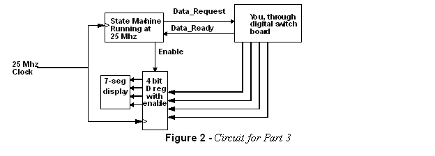
Build your state machine using Verilog, but construct your D-register using the schematic editor, and connect the state machine to the register using the graphic schematic editor.
- You are to design a finite state machine that controls the circuit of Figure 3, and interacts with you as the user. This is the same circuit that you implemented in Lab 5, part 5. The clock signal (for both the finite state machine and the Registers A and B) will be connected to the 50MHz (period 20ns) clock signal that is generated on the DE2 Educational board.
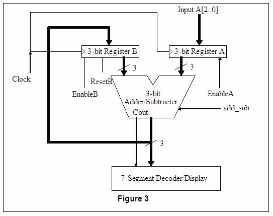
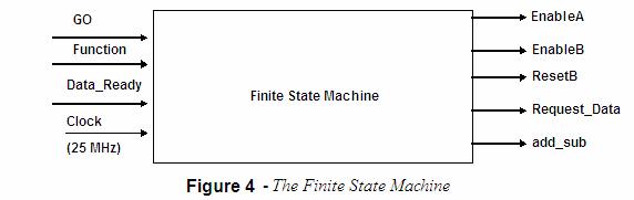
The outputs of the finite state machine (illustrated in Figure 4) are:
i. EnableA - the enable signal for register A. When this is turned on, register A will, on the next positive edge of the clock, copy the input data A[2..0], coming from user switches into register A.
ii. EnableB - the enable signal for register B. When this is turned on, register B will, on the next positive edge of the clock, copy the output of the adder/ subtracter into register B.
iii. ResetB - an active-low signal which should set the contents of register B to zero. Make this a synchronous reset.
iv. Request_Data - is an output (to be hooked up to a light on the digital switch board) which will signal to you that the machine wants you to input data.
v. add_sub - is connected to the add_sub signal of the adder/subtracter, to tell it which function to perform. (=1 means add, =0 means subtract)
The inputs of the finite state machine are:
i. GO - active low (i.e. active when signal = 0). When activated, this causes the machine to begin operation, as described below.
ii. Function - this is an input from the user which indicates the “instruction” that is desired. Function = 1 means that the two numbers should be added. Function =0 means that the two numbers should be subtracted.
iii. Data_Ready - this signal should be connected to a switch on the switch board. It is the other part (with Request_Data) of the handshake between you and the state machine. Once the data is ready, you raise the Data_Ready signal. Once the Request_Data signal is lowered, you must lower the Data_Ready signal.
When the GO signal is activated, your machine should request two pieces of 3-bit data from the user (one at a time) and either add or subtract them, depending on the Function input. To obtain the two pieces of data, you must use the handshaking protocol described above in the background section. Code your Finite state machine in Verliog. Turn it into a symbol and connect it to the circuit of Figure 2 using the schematic editor.
4.0 In the Lab
- Build and test the circuit from part 1 of the preparation.
- Build and test the circuit from part 2 of the preparation. You must use the logic analyzer to show the sequence of transitions in this high-speed circuit.
- Build and test the circuit from part 3 of the preparation.