ECE241F - Digital Systems - Lab 7
Complex Finite State Machines and Digital Hardware Displays
1.0 Purpose
In this lab you will see how to display images on a computer-type monitor and how to change them pixel-by-pixel. You’ll be doing this in hardware, without any software, with the help of a hardware module that we will give you called the “VGA Adapter.” VGA, which stands for “Video Graphics Array” is a standard for sending signals to a display that cause the pictures you see on most displays. The adapter hides most of the inner workings of the actual monitor and provides a simple interface so that you can use it in your digital circuit.
This lab demonstrates two key methods of how to create pictures on the display in hardware: First, it shows how to create the initial background image the adapter displays on screen. Then, the lab walks you through a design of a simple “etch-a-sketch” (http://www.etch-a-sketch.com/) circuit that allows you to draw arbitrary shapes by drawing dots on the screen.
2.0 Background
1. In Labs #5 and 6, you created and controlled an adder which had the capability of adding or subtracting two numbers. In this lab you will again need to use an adder/subtracter; you may again use the LPM function available in Quartus for this.
2. In Lab #6, you created a Finite State Machine (FSM) that controlled an adder and the seven segment decoder based on inputs from external switches as well as the current state. You should now be able to construct a finitie state machine that determines the outputs based on the current state and external inputs.
3. In class, you were given a description of the basics of how the VGA adapter works. You should also read the information about the VGA adapter provided at http://www.eecg.utoronto.ca/~jayar/ece241_06F/vga/. First read the page titled “VGA Adapter Basics” and then “VGA Adapters Interface.”
3.0 Preparation
Part A: Create a Background Picture
The VGA adapter module can be initialized to have a “background” picture that a circuit can subsequently change by writing into separate super pixels. In this part, we will describe how to create that background picture.
The first thing to know is that the picture being displayed on the screen by the adapter is stored in memory that is internal to the adapter. The Quartus software and the FPGA hardware allow this memory to be initialized (i.e. set to some initial value) when then device is first programmed. Memory initialization is done by creating a “MIF” file (for “memory initialization file”).
In this part of the lab you will learn how to set that initial image to one that you draw using a simple drawing program.
- First, draw an image you would like to display when you first program your design onto the DE2 board. Create this image using the Microsoft Windows “Paint” program, in the following way:
- Start the Paint program, typically available from the Start Menu: that is Start->Programs->Accessories->Paint
- Select the menu item Image->Attributes. In the dialog box set “width” equal to 160 and “height” equal to 120, as this is the resolution of the monitor that the adapter uses. Select “pixels” as the unit. Select “colours” as well.
- Draw a picture of your own design; use simple colours like Red, Green and Blue.
- Once the image is complete, press Ctrl-A to select the entire drawing and then select Image->Flip/Rotate option from the menu. When a new window pops up, select “Flip vertical” and click OK.
- Save the file, using File->Save As and save it as a 24-colour bitmap image.bmp.
- Download the program bmp2mif.exe from the location: http://www.eecg.utoronto.ca/~jayar/ece241_06F/vga/bmp2mif.exe or just go to the download section of the website. Put this program in the folder where your image.bmp file is. Run a DOS command shell (by going to Start->Run and running “cmd” in windows XP) and execute the command “bmp2mif image.bmp” without the quotes. This will produce the files image.colour.mif and image.mono.mif, which you will use next.
- Download a copy of the VGA Adapter from the download web page or from http://www.eecg.utoronto.ca/~jayar/ece241_06F/vga/VGA_Shell.zip to a folder named PartA. Copy the image.colour.mif you created in the previous step into that directory. Rename the image.colour.mif to display.mif. Compile it in the normal way to be ready for download – that’s it! In the lab when you will download this circuit into the board, you should be able to see your picture on the VGA monitor.
Note that the procedure described above only sets the picture displayed on the monitor after you initially program the DE2 board with the design. It does this by initializing the memory used in the adapter.
Part B: Etch-a-Sketch
In this part you will learn how to draw new super pixels on the screen after your circuit begins running. To demonstrate this, you will design a simple “Etch-a-Sketch” -like drawing system.
This will be a circuit that moves a cursor around the screen, either up, down, left, or right, and draws a new pixel with every move the cursor makes. The system has 6 inputs, described below, and the output is provided by the VGA controller and appears on the screen. The inputs are:
· Resetn – an active low input to reset the system. Reset should cause the cursor to go to position (0,0) the top-left corner of the screen.
· CLOCK_50 – the clock input to drive the finite state machine of the system as well as the VGA adapter.
· Four switches labelled Left, right, up, down – to indicate the direction to move the cursor in. Each time an input, for example “Left” is set to 1, the drawing system show move the cursor left by exactly 1 pixel. (It should wait until the Left signal returns to 0 before moving the cursor again).
The basic design of the circuit for the etch-a-sketch system is given in Figure 1. It contains 3 major blocks:
1. The VGA adapter responsible for the drawing of pixels on the screen. See the website above for a description of how the adapter works.
2. The datapath that controls the position of the cursor, providing the VGA adapter with the (X,Y) (i.e. column, row) location where a pixel should be drawn
3. A finite state machine that receives the input from a user and directs the datapath to change the position of the cursor accordingly, by adding and/or subtracting from the (X,Y) position of the cursor.
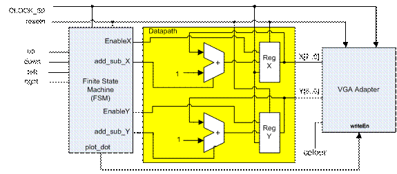
Figure 1 – Design Overview – State Machine, Datapath and VGA Adapter
To implement the etch-a-sketch game as described above complete the following steps:
- Download a copy of the VGA adapter into directory named PartB from http://www.eecg.utoronto.ca/~jayar/ece241_06F/vga/VGA_Shell.zip, and start Quartus by double clicking on the project file DE2_TOP.
- Create the datapath as shown in Figure 1 using the schematic editor. Do not use Verilog for the top-level module. To create the adder/subtracter you should use the LPM_ADD_SUB module. To place down a copy of the VGA Adapter module, bring up the schematic library as usual in the schematic editor. There will be a library called “Project” that you should open, and in there will be the symbol called VgaAdapter, which you can place in your schematic as usual.
- Create a finite state machine to control the datapath shown in Figure 1. You should use Verilog to create the finite state machine – turn it into a symbol and place it into the schematic. It should take all four user inputs and produce outputs EnableX, EnableY, add_sub_X, add_sub_Y and plot_dot. The FSM should have 5 states:
i. Reset state – initial state where the FSM resets the X and Y registers to 0. The reset signal is asynchronous.
ii. Wait state – wait for user to toggle one of the left, right, up or down switches
iii. Move cursor – change the position of the cursor by enabling register X or Y and incrementing/decrementing its value
iv. Plot – enable plot_dot signal and go to the final state
v. De-assert – wait for the user to put all switches in the down (off) position before proceeding back to the wait state.
- Connect the three components as shown in Figure 1. The colour input of the VGA adapter should be set to a constant value, something other than all zeroes. Pick your favourite colour!
- You may wish to simulate parts of your circuit before the laboratory, such as the adder/subtracter and the finite state machine. You will have to do this separately from the VGA adapter because there is no way to sensibly observe its output in simulation, which will also take many cycles to produce.
4.0 In the Lab
The teaching assistants will show you how to physically connect the Altera DE2 board’s VGA output to the VGA Cable from the KVM switch so that you can see the display output on the computer monitor. This will include a number of connections that must be in place for the KVM switch to work correctly.
Be sure that your design connects all the Clock signals of your design to the 50 MHz DE2 Onboard Clock.
1. Download the Circuit from the preparation Part A into the DE2 board. Switch the KVM switch to display the output from the DE2 board. If the VGA monitor is connected correctly, you should see the picture that you drew in the Paint program on the display.
2. Download and test your circuit from Part B.
3. Optional: If you have time, use the background image you used in Part A (the file image.colour.mif replacing the display.mif file) as the background for the circuit of Part B by recompiling Part B with the different display.mif file.