Lecture 3
Andreas Moshovos
Spring 2004, revised Spring 2006
General Notes on
Programming Model and Implementation
In what follows we focus on describing how various computer units behave (their operation model).
The operation model of a unit is a specification of how this unit interacts with the outside world. The model includes: (1) the types of operations that the unit is capable of performing, (2) how one should specify the desired operation, and (3) what the outcome would be. It says nothing about *how* the unit is supposed to perform these operations. The operation model should be viewed as contract between the manufacturer and the user.
An implementation is correct only and only if it behaves in accordance to the operation model.
The key advantage of this division between implementation and the operation model is that the manufacturer and the programmer can proceed independently in their respective tasks. The manufacturer can design different implementations that adhere to the operation model while proving different cost, complexity and performance characteristics. She can also take advantage of advances in technology as these become available. At the same time, the programmer can write programs and expect these to behave correctly on new implementations as long as these implementations adhere to the operation model.
The more one includes into the operation model the more restrictive it becomes. It is best to strike a balance between functionality and specifics. For example, the operation model could specify that the operation ADD X, Y adds the two numbers X and Y and places the result in X. It could also specify that this operation will complete in 100ns. However, this is a not a very good idea as it imposes an additional constraint.
To understand the difference between specification and implementation consider the NAND gate. A possible way to specify what the NAND gate does is via a truth table. Assuming that 0 and 1 are represented using voltages then two possible implementations are via transistors or via a person hidden into a box (we will explain during the lecture).
Memory
What is Memory: Its purpose is to store data and instructions that are manipulated and executed by the computer.
In its fundamental form memory is a vector where each element is in most cases a byte (8 bits).
Each memory location has two attributes: (1) an address and (2) its contents. Both of them are *numbers*.
(note to self :) draw figure of memory with addresses and contents. Show the address and the contents of a location.)
The address of each memory location is fixed at manufacturing time and cannot be altered. Each memory location has a unique address. Addresses typically start at 0 and grow arithmetically, i.e., the first byte is at address 0, the second at address 1, and so on.
The collection of all addresses is called the address space. Typically the address space is a power of 2. In the processor we will be using the address space is 16Mbytes or 2^24. Other modern processors use 2^32 (4 Gbytes) and the recent 64-bit processors have an address space of 2^64 (very very large).
The contents of each memory location can be changed/read at will.
Memory supports two operations:
1. Read/Load à Reading the contents of a location
2. Write/Store à Changing the contents of a location
Load: Takes the form “Load ADDRESS” e.g., Load 0xfe. This operation returns the contents at memory location/address 0xfe ($fe in 68K assembly). Show example with figure.
Store: Takes the form “Store Data, ADDRESS” e.g., Store, 0xf0, 0x10. This operation changes the contents of memory location 0x10 to 0xf0. The existing value in that memory location is lost and replaced with 0xf0.
Note: The typical memory behavior model defines that the outcome of a sequence of memory operation is such that as if the memory operations where performed one at the time in their entirety and in the order they appeared. E.g., if we perform “store 0x10, 0xf0” and then “store 0x20, 0xf0” then at the end memory should behave in such a way so that memory location 0xf0 holds the value 0x20 and not 0x10. This may appear pretty obvious but many of the performance enhancing techniques rely heavily on dissecting this model down to the bare minimum. This is the sequential execution model that pretty much everyone has learned to program with. If you think about it this is the way you reason for what a C program is supposed to do. When memory adheres to the sequential execution model, each operation is said to be atomic. That is, it gets performed on its own with no interaction or overlap with any other operation.
Note this is just a behavior model, the actual implementation may be different.
So what will be the content of memory and the outcome of the following sequence of instructions assuming memory is initially filled will zeroes?
1. STORE 0x1, 0xfe
2. store 0x2, 0xfe
3. load 0xff
4. load 0xfe
5. store 0x3, 0xfe
1 changes the contents at address 0xfe to 1
2 changes the contents at address 0xfe to 2
3 returns 0
4 returns 2
5 changes the contents at address 0xfe to 3
For convenience and practicality memories also support reading other data types except a byte. In 68k and in most modern machines one can access a single byte, two bytes (a word in 68k terminology) or four bytes (a long word in 68k terminology)
68k terminology
1 byte / Symbol .b
2 bytes = word / Symbol .w
4 bytes = long word / Symbol .l
In this case we have to extend our vocabulary from simple LOAD and STORE to a combination of operation and data type. Thus we have:
Load.b Address
Load.w address
Load.l address
Store.b byte, address
Store.w word, address (2 bytes)
Store.l longword, address (4 bytes)
In this case it is convenient to draw memory as an array where each row comprises four consecutive bytes.
|
0x00 0000 |
0x11 |
0x22 |
0x33 |
0x44 |
|
0x00 0004 |
0xff |
0x88 |
0x62 |
0x51 |
|
. . . |
|
|
|
|
|
0xff ffff |
|
|
|
|
Let’s see a couple of examples:
a. Load.b 0x000000 à returns 0x11
b. Load.b 0x000003 à returns 0x44
c. Load.w 0x000000 à returns 0x1122
d. Load.l 0x000000 à returns 0x11223344
e. Load.w 0x000006 à returns 0x6251
All aforementioned operations are aligned. A memory access is aligned if the address it accesses is divisible by the size of its data type. Thus all byte accesses are aligned since all addresses are divisible by sizeof(byte)=1. A word access is aligned if the address is even (divisible by 2). Finally, a long word access is aligned if the address is divisible by 4. Note that a number is divisible by 4 if in its binary representation the last two least significant bits (i.e., the ones on the right) are both 0.
An access is unaligned if it is not aligned :). Different architectures impose different constraints on whether accesses have to be aligned or not. For example, in 68k all accesses must be aligned same in most modern architectures. In x86 (Pentium 4) accesses do not have to be aligned. The benefit of allowing unaligned accesses is “ease” of programming (not really all that compelling). The benefit of not allowing unaligned accesses is ease of implementation (could explain in class or ask me).
Endianess
Computers and their components and thus memories were
defined and built by humans from scratch. And whenever humans have to choose
amongst several options chances are that different people will choose
differently. A prime example of this is the issue of Endianess.
Endianness = when I read multiple bytes from memory to form a larger data type (e.g., a word or a long word) in what order do I assemble the bytes into the larger data type?
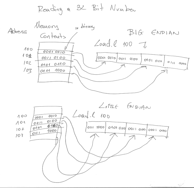
Before we said that load.l 0x000000 returns 0x11223344. This is called BIG-ENDIAN. This is because the first byte we read (that at the first address of 0x0000000) is placed on the “big” (i.e., most significant) side of the word.
There are machines where the opposite is true. That is in machines that are LITTLE-ENDIAN load.l 0x000000 would return 0x44332211.
68k is big-endian. X86 is little-endian. Other machines are BI-ENDIAN that is we can program them to behave as little or big endian at will. However, at any given point of time the machine will be operating at one of the two modes.
There is no particular reason why is one better than the other.
Note that the internet (i.e., the IP protocol) is BIG-ENDIAN.
The following figure shows an example of a “load.l 100” for big and little endian memory systems. The contents of memory locations 100 through 103 are shown in binary.
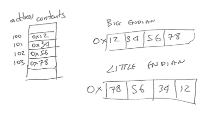
The following figure repeats the previous example but now we use a hexadecimal notation to avoid writing each bit. Please note that memory still operates at the binary level. This is just a convenient shorthand notation. There are no hexadecimal numbers anywhere in memory.
A note about
addresses and contents:
You can never change the address of a memory location. It’s fixed at design time. For example, there is only one address called 100 and it is always the same one no matter what. You can change only change the contents at each memory location. However, because, addresses and contents are numbers you can read a number from the contents of a memory address and then use that number as an address to refer to some other memory location. This is what pointers do. We will explain this further when we talk about pointers.
------------------------------------------------------------------------------------
A physical
interface to a memory device:
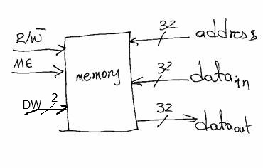
And in order to not forget that we eventually we will be talking about actual implementations let’s see how a typical memory interface will look at the physical level. This exercise will allow us to see how we can use the binary system to encode quantities other than numbers.
So, let’s start first with the vocabulary we need to be able to talk. This includes the operations and their arguments. Our goal is here to determine how many signals (i.e., bits) we will need to be able to specific these operations. We have the following operations:
1. Load.DataType Address
2. Store.DataType Data, Address
Where DataType can be any of the following three: byte, word or long-word. Address is 24 bits for 64k. And Data can be 8, 16 or 32 bits.
These requirements can be stated as follows:
1. Two operations: Load or store
2. Three data types: byte, word or long-word
3. One address of 24 bits
4. One data value of at *most* 32 bits for specifying the value to write for stores
5. One data value of at *most* 32 bits for memory to returns the value for loads
6. We also need to be able to say that we do not want to read or write from/to memory, i.e., do nothing
For 1 it’s enough to use a single signal which we will call R/W’. When R/W’ = 1 then we want to perform a load, while when R/W’ = 0.
For 2, it’s enough to use two signals. Let’s call them
collectively DW and use the following encoding (others possible):
DW | Data Type
----------------
00 | byte
01 | word
10 | not used
11 | long-word
For 3 and 4 we need 32 signals for each (or we could multiplex the same wires).
Finally for 5 we need a master-enable signal ME. When ME = 0 memory ignores all other signals. When ME = 1 then memory looks at the other signals and responds accordingly.
Here’s the physical interface of our memory:
Besides being able to say to memory “do noting” ME plays another important role. In the physical world it takes time for us to setup coherent values on all signals. For example, assume we want to perform in sequence a STORE.BYTE 0x10, 0X000000 and a STORE.BYTE 0x01, 0xffffff. It is practically impossible to change all signals instantaneously. So, in going from address 0x000000 to 0xffffff all possible binary numbers may temporarily appear (because different signals may change at different rates). Without the ME, the memory could get confused and misinterpret the second store. With ME, we can se ME to zero in between the two stores, wait sufficient time for the second store values to appear on the data and address signals and then set ME=1. This way memory remains oblivious to temporarily inconsistent values.
Multiplexing data_in and data_out
In our preceding design two separate sets of 32 wires each were used for reading and for writing data from and to memory respectively. Often times, the number of pins available per chip is limited by cost (a integrated circuit becomes increasingly and significantly more expensive the more pins it uses). Accordingly, designers often try to find ways to reduce the number of external connections (pins). In our memory we could “multiplex” the data_in and data_out signals. This does not violate the behavioral model as it does not support simultaneous reads and writes. We can only read or write but not both at the same time.
One way of multiplexing these wires is via the use of tri-state buffers. The symbol/connections for a tri-state buffer and it’s truth table are as follows:
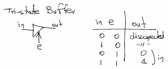
When the e input is zero the in and out terminals are as if they are completely disconnected. Using 32 tri-state buffers one per data bit we can multiplex the data_in and data_out signals as follows:
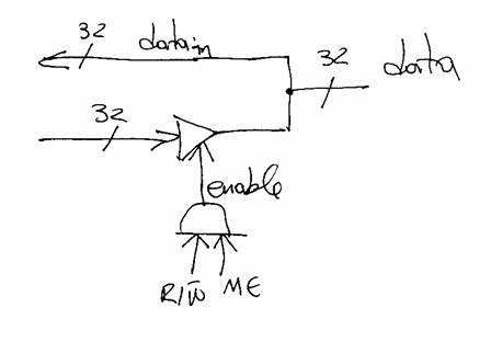
Only when we do a read (R/W’ = 1 and ME = 1), the tri-state buffers are enabled and memory “drives” (i.e., places a value) on the data wires. In all other cases, the data wires behave as inputs so they can be freely set to any value desired (i.e., when doing a write).
Using this methodology we can build a bus where multiple devices are connected to the same set of wires and by appropriately enabling their outputs we can make sure that only one device is “driving” (i.e., placing a value) on the bus and others (one or many) are reading it. As a side-note, please keep in mind that these busses do not scale very well primarily as a result of increased parasitic capacitance on the wires.
Practice
questions/topics:
1. If you are given a memory that supports only reads and writes for bytes can you synthesize one that also supports reading and writing a word (i.e., 16 bits or 2 bytes)?
2. If you are given a memory that supports only reads/writes for words (two bytes) can you synthesize one that also supports reading and writing a byte?
Hint: Think about doing this in multiple steps/accesses. Recall, the memory behavioral model says nothing about *how long* it will take for an operation to complete.