Lecture 15
Andreas Moshovos
Introduction to
Devices – A Parallel Interface
Having discussed instructions and how these can be used to manipulate data in memory and registers we now move on to how a processor can interact with the physical world via devices. If you recall in our first lecture we explained that what makes computers really useful is that they can, with the help of specialized devices, interact with the physical world.
Following the same approach as the one we used for explaining machine instructions, memory and registers we will first discuss the programming model for a specific device. That is, initially we will ignore how the device works, and focus on how it behaves. Initially, for us the device will be a black box which we can program following the programming model. Later on we will discuss the implementation of the device. This how it works and as we explained earlier, there may be many different implementations that adhere to the programming model.
The difficulty with devices is that there isn’t a universal programming model that can be applied to all devices. While there may be some minor similarities, for the most part most devices are specialized units and their programming model differs significantly from that of other devices. For this reason, we will start with a specific example and then point to some underlying principles that are used by most devices. The example we will use is a parallel interface (PIT).
Before we proceed to discuss the PIT as it is used in the Ultragizmo board we will first discuss how the processor can talk to the PIT and read or write data from/to it. For this purpose let us first define the term name space. A name space is a set of names that the processor can access (read from or write to) using instructions. Thus far we have seen two name spaces: memory and registers. In 68k the memory name space (the address space) comprises 4G different addresses while the register name space includes D0-D7 and A0-A7. In many processors and computers that exist today, the memory name space is also used to refer to devices. That is, some memory addresses are reserved (at design time) for accessing I/O (input/output) devices. Accessing devices this way can be done using the same instructions that access memory (e.g., move.l). In some processors there is a separate name space for accessing devices. A notable example is the x86 family (Pentium 4 belongs in this family) where there are three name spaces: (1) registers, (2) memory and devices. In such machines, there are additional instructions for accessing devices (called IN and OUT in x86). Today it makes little sense to have a different name space for devices. Thus, most processors and computers today use MEMORY MAPPED I/O. In memory mapped I/O devices appear as memory locations and can be accessed using the same instructions that access memory. We will later explain how memory mapped I/O works (the physical design). For the time being suffices to consider that some addresses are NOT mapped to memory elements but to devices.
The Parallel
Interface Programming Model
On the Ultragizmo board there is a parallel port device. This device provides eight external connections. Each connection is a single wire which can be used as input or output. Under program control we can either read the logical level at each of those wires (i.e., whether the voltage on that wire is a logical 1 or a logical 0) or set their voltage to logical 0 or logical 1.
As an example we will consider an application where the PIT is used to control the fan of a heating system. The PIT will be used to read the status of a thermostat and then it will be used to turn on or off the heating system’s fan. We will assume that the thermostat provides a single output which is 0 if the temperature is less than a preset level and 1 otherwise. We want to turn of the fan if the thermostat’s output is 0 and turn it off otherwise (you may observe that a computer is probably an overkill for this application, however, please recall this is an example). So, one of eight PIT connections will be used as input to read the thermostat status and another will be used as output to control the fan motor.
The PIT interface presents a programming interface that consists of three bytes in memory:
1. The DATA DIRECTION register (DDR) which can be accessed via memory address $C10002
2. The DATA OUTPUT register (DOR) at address $C10000
3. The DATA INPUT register (DIR) at address $C10004
|
Address |
BYTE |
|
|
$C10000 |
DOR |
Data Output Register |
|
|
|
|
|
$C10002 |
DDR |
Data Direction Register |
|
|
|
|
|
$C10004 |
DIR |
Data Input Register |
As we noted earlier the PIT provides eight external single “bit” (wire) connections to the outside world. Let’s us call these connections PIT0 through PIT7.
Each of these connections can be configured as an input or an output independently. This can be done by writing a value into the DDR register. The DDR register has eight bits which we can change via the aforementioned address. Each of these bits control the direction of the corresponding external connection. For example, if bit 0 of DDR is set to 1, then PIT0 becomes an output otherwise it becomes an input. Note that DDR can only be written into. It cannot be read. We can still try to access the memory location DDR lives in, but the value that we are going to read is for all practical purposes unknown (we may get a specific value on the Ultragizmo board but this is an implementation feature, a future implementation of Ultragismo may safely behave differently).
Example: the instruction move.b #FF, $C10002 configures all PIT connections as outputs. Move.b #0F, $c10002 configures PIT0 through PIT3 as outputs and PIT4 through PIT7 as inputs.
To set the value of a PIT bit to a specific level we have to write into the DOR
register. Thus, assuming that DDR=$FF, then writing $0F into DOR forces
PIT0-PIT3 to logical 1 and PIT4-PIT7 to logical 0.
At any time we can access the DIR register and read the logical values of the eight external connections. If a connection has been configured as an output we are effectively reading the value written in the corresponding bit of the DOR. If a connection has been configured as an input then we are directly reading whatever value has been placed on the connection from the outside world (for example from the thermostat).
Example: Let’s us now write the program that reads the thermostat and controls the heating fan. We will assume that the thermostat is connected to bit 0 of the PIT (which should be configured as an input) whereas the fan is connected to bit 2 (which should be configured as an output). So:
PIT0 is connected to the thermostat’s output
PIT2 is connected to the heat fan motor
DDR equ $C10002
DOR equ $C10000
DIR equ $C10004
org $20000
heat
move.b #$04, DDR ; configure all but PIT2 as inputs
move.b #$00, DDO ; turn the fan off (only bit 2 is important)
fever
move.b DIR, d0 ; read PIT
and.b #$01, d0 ; hold only bit 0
beq fanon ; if it is zero then turn fan on
move.b #$0, DDO ; turn the fan off
bra fever
fanon
move.b #$4, DDO ; turn the fan off
bra fever
In order not to forget that C provides us with most of the functionality that assembly does the above code can also be written directly in C:
#define DDR ((unsigned char *) 0xC10002)
#define DDO ((unsigned char *) 0xC10000)
#define DIR ((unsigned char *) 0xC10004)
void
heat (void)
{
unsigned char t;
*DDR = 0x04;
*DDO = 0x00;
while (1)
{
t = *DIR;
if (t & 0x1)
*DDO = 0x0;
else *DDO = 0x04;
}
}
So, while programming try to avoid using assembly as much as possible. In most cases this will be possible. However, there are cases where using assembly will be important and necessary (for example, you have little control of how the compiler translates a piece of C code, hence it may use inefficient instruction sequences, moreover, since the compiler does not have an understanding of device semantics – programming model – it may use instruction sequences that have unexpected behavior such as accessing the same device register multiple times).
As an additional example let us consider what happens when the thermostat uses a mechanical arrangement where metal contacts touch to report a logical 1. Whenever metal contacts are used there is a short period of time where they bounce repeatedly whenever the switch changes state. So for a short period of time what we will observe at thermostat’s output will be a series of alternating 0’s and 1’s. The 68k is much faster in processing instructions hence the above code will turn on and off the fan several times while the thermostat changes state. We can revise our program to reduce this or even avoid it completely. This is typically called debouching. Here’s one way of achieving this: Rather than reading the DIR once (taking a single sample of the input’s state) we read it several times counting how many times it was 1. If we took N samples and the number of those samples that was one is greater than N/2 then we can assume that the value read is 1 otherwise we can assume it is a zero. Here’s the code:
DDR equ $310002
DOR equ $310000
DIR equ $310004
org $20000
heat
move.b $04, DDR ; configure all but PIT2 as inputs
move.b $00, DDO ; turn the fan off (only bit 2 is important)
fever
clr.l d1 ; d1 will be used to count the 1 samples
move.w #1000, d2 ; take 1001 samples
sample
move.b DIR, d0 ; read PIT
and.b #$01, d0 ; hold only bit 0
add.l d0,d1 ; if it was one increment d1
dbf d2, sample
cmp.l #500, d1
bge fanoff ; if more than 500 samples where 1 then assume this is a 1
move.b #$0, DDO ; turn the fan off
bra fever
fanon
move.b #$4, DDO ; turn the fan on
bra fever
Please note that I have not tested this code on the Ultragizmo so, using 1000
may not be the best possible choice or even a good one.
The PIT
Implementation
Having seen how to program the PIT we can now discuss one implementation. At the physical level the PIT presents the following signals:
1. Data: a set of 8 wires that are used for supplying the value to written to registers DDR or DDO, or to read the value from the DIR. These signals can be used as input or as output as explained subsequently.
2. A DDR write signal: When this is 1 the value in the Data is written into the DDR
3. A DDO write signal: When this is 1 the value in the Data is written into the DDO
4. A DIR read signal: When this is 1 the Data signals are placed in output mode and their take the values that currently appear on the external port connections
5.
The circuit for the Ultragizmo implementation of PIT is shown in figure 23 of the ultragizmo manual. For the time being let us ignore the connections to the signals A1-A23, D0 and R/W since these are the signals used for interfacing with memory in general (see discussion that follows).
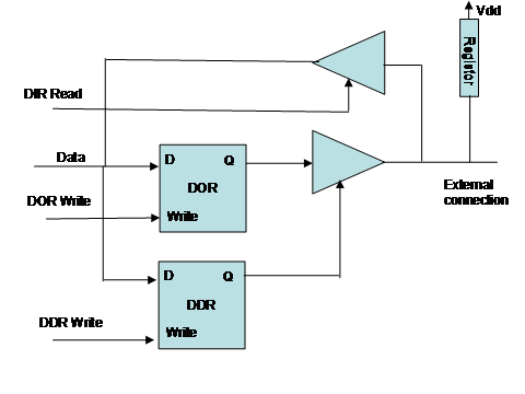
The DOR and DDR boxes are Latches. We can change their value using the Data and Write signals. The DDR latch output drives a tri-state driver whose output is connected to the external connection. If DDR is 1 then the tri-state buffer behaves like a buffer and passes the value of the DOR latch to the external connection. If DDR is 0 then the tri-state buffer is placed in the off state which can be thought as an open switch (no connection). In this case, an external source will determine what the value is on the external connection wire. The resistor is there to help when DOR wants to drive a 1 (high voltage) since the technology used is not very “strong” when driving a one. The registor also sets the external connection to 1 when no one is driving it.
If DIR Read becomes 1 then the upper tri-state buffer is activated and passes the value on the external connection wire to the data wire. What we have described is just one of the 8 slices used by the PIT. The 8 slices are connected together so that they share the Write and Read lines and so that their data lines collectively form the 8-bit data interface of the PIT.
To connect the PIT to the 68k system we need to first explain what is the physical memory interface. This discussion follows. We do not discuss the exact implementation in 68k. Instead we present an interface that is simple enough to allow us to focus on the fundamentals.
Interfacing with
Memory
------------------------------------------------------------------------------------
And in order to not forget that we eventually we will be talking about actual implementations let’s see how a typical memory interface will look at the physical level. This exercise will allow us to see how we can use the binary system to encode quantities other than numbers.
So, let’s start first with the vocabulary we need to be able to talk. This includes the operations and their arguments. Our goal is here to determine how many signals (i.e., bits) we will need to be able to specific these operations. We have the following operations:
1. Load.DataType Address
2. Store.DataType Data, Address
Where DataType can be any of the following three: byte, word or long-word. Address is 24 bits for 64k. And Data can be 8, 16 or 32 bits.
These requirements can be stated as follows:
1. Two operations: Load or store
2. Three data types: byte, word or long-word
3. One address of 24 bits
4. One data value of at *most* 32 bits for specifying the value to write for stores
5. One data value of at *most* 32 bits for memory to returns the value for loads
6. We also need to be able to say that we do not want to read or write from/to memory, i.e., do nothing
For 1 it’s enough to use a single signal which we will call R/W’. When R/W’ = 1 then we want to perform a load, while when R/W’ = 0 we perform a store (write to memory).
For 2, it’s enough to use two signals. Let’s call them
collectively DW and use the following encoding (others possible):
DW | Data Type
----------------
00 | byte
01 | word
10 | not used
11 | long-word
For 3 we need 24 signals.
For 4 and 5 we need 32 signals for each (or we could multiplex the same wires).
Finally for 5 we need a master-enable signal ME. When ME = 0 memory ignores all other signals. When ME = 1 then memory looks at the other signals and responds accordingly.
Besides being able to say to memory “do noting” ME plays another important role. In the physical world it takes time for us to setup coherent values on all signals. For example, assume we want to perform in sequence a STORE.BYTE 0x10, 0X000000 and a STORE.BYTE 0x01, 0xffffff. It is practically impossible to change all signals instantaneously. So, in going from address 0x000000 to 0xffffff all possible binary numbers may temporarily appear (because different signals may change at different rates). Without the ME, the memory could get confused and misinterpret the second store. With ME, we can se ME to zero in between the two stores, wait sufficient time for the second store values to appear on the data and address signals and then set ME=1. This way memory remains oblivious to temporarily inconsistent values.
Connecting the PIT
to the Memory Interface
----------------------------------------------------------------------------------------------------
To connect the PIT to the memory interface described previously, we first connect the PIT Data lines to the lower byte (8 bits) of the memory data lines. This will allow us to access the three PIT elements (DDR, DOR and DIR) by using load byte and store byte memory accesses. Then we need to activate the corresponding PIT elements depending on the address accessed. We need to detect the following combinations on the address lines: $310002, $310004 and $310000. In the simplest to describe implementation we use a 32 input AND gate for each of those. Let’s see how we decode the address $00310000. For this we will connect lines A21, A20 and A16 directly to the AND gate. The rest 29 address lines are connected to the AND gate after they are reversed. The net effect is that the AND output becomes 1 only when the address is $00310000. If we AND this with NOT R/W and MasterEnable then we get the DOR write signal. A similar methodology can be used to design the circuits that drive the other two signals (DDR write and DIR Read).
Here’s the ADDRESS DECODING part. This is the circuit that generates the DORwrite, DDR_write and DIR_read signals. The DATA lines are connected directly to the corresponding PIT data lines
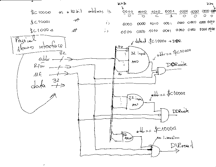
We are using three 32-input AND gates. Each is connected to all 32 address signals. By using inverters appropriately we can detect that the address being accessed is one of those mapped to DOR, DDR and DIR. We start by looking at the binary representation of these addresses and put an inverter for those address bits that are zero in the pattern we are interested in. After detecting the address, we then use a 3-input AND gate to detect accordingly whether an access is being made (ME == 1 – ME is Master Enable), and whether it is a read or a write. We care for Writes for the DOR and DDR and for reads for DIR.
This implementation is easy to understand, however, it’s not necessarily the most efficient. This topic is beyond the scope of this lecture, however, you are encouraged to think of ways of reducing the number of components needed to do address decoding.
Here’s the complete design:
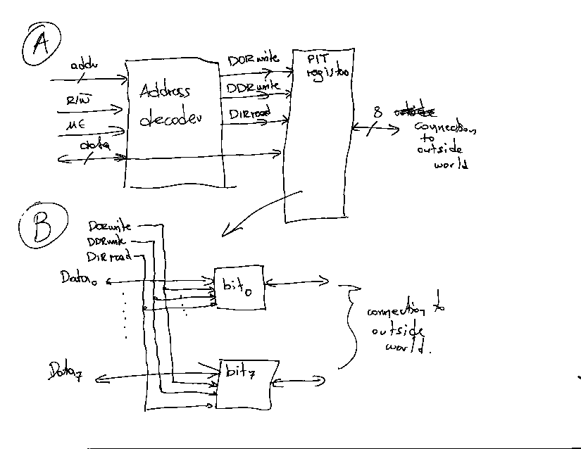
Each bit cell (there are eight of them) is as shown earlier):