Microprogrammed
Control
Andreas Moshovos
Spring 2007
As we have seen, the control unit of the multi-cycle implementation is a finite state machine, or FSM. Given a description of an FSM it is possible using digital design methodologies to implement the FSM as a digital circuit. The implementation we have seen is hardwired, that is it corresponds to one specific FSM. If we were to make changes we will have to redesign the implementation. In this lecture we will be discussing a different implementation of control FSMs. The key characteristic of this implementation is the ability to make some changes in the FSM. This implementation is called microprogrammed control, as the same exact hardware can be used to implement many different FSMs. In a way, given an FSM, the hardware can be programmed to implement it.
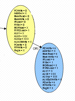
So, our goal here is to design a circuit that can be used to implement many different FSMs. Let us start by first discussing what an FSM does. Let us look at one of the state transitions. The next diagram shows the state transition from cycle 2 to cycle 3 for the ORI instruction.
To implement an FSM we need to be able to:
- Remember what state we are in.
- Set values for all datapath control signals.
- Specify what is the next state.
The following figure shows the components of an example microprogram control unit:
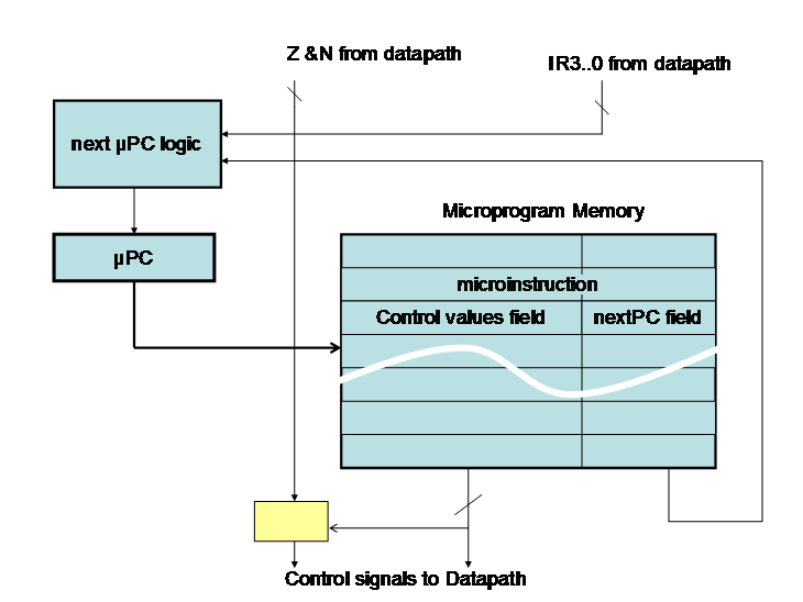
There are three major components;
- The microprogram memory.
- The microPC.
- The next microPC logic.
The microPC serves a dual purpose. Its value identifies the current FSM state. So, with it we can remember which FSM state we are at. It is also used as an address to read a row from the microprogram memory. The microprogram memory implements the other two functions of the FSM: setting values for the datapath control signals and the next state transitions. The microprogram memory remain constant while the processor is executing instructions. However, by changing its contents we can change the control FSM. So, this implementation allows some flexibility in changing the FSM.
Each row of the microprogram memory contains a microinstruction. Each microinstuction corresponds to a unique FSM state. The microinstruction has two fields:
- The datapath control values. These are used to set the control signal values for the datapath. Accordingly, by programming these bits we can implement any combination of control signal values. As we will soon explain, some datapath control signals also use the Z and N flags in addition to the microinstruction values (yellow box).
- The next microPC selection field. This is fed to the next microPC logic which determines which is the next state. Effectively, this determines the state transitions. Again, by changing this field we can change the state transitions.
Here’s the format of the datapth control values field:
|
PCwrite |
AddrSel |
MemRead |
MemWrite |
IRload |
R1Sel |
MDRload |
R1R2load |
ALU1 |
ALU2 |
ALUop |
RFWrite |
RegIn |
ALUOutWrite |
FlagWrite |
Notice that for each datapath control signal there is a field in the microinstruction.
To implement cycle 1 we will use the following microinstruction:
|
PCwrite |
AddrSel |
MemRead |
MemWrite |
IRload |
R1Sel |
MDRload |
R1R2load |
ALU1 |
ALU2 |
ALUop |
RFWrite |
RegIn |
ALUOutWrite |
FlagWrite |
|
1 |
1 |
1 |
0 |
1 |
0 |
0 |
0 |
0 |
001 |
000 |
0 |
0 |
0 |
0 |
To implement cycle 2 we will use the following microinstruction:
|
PCwrite |
AddrSel |
MemRead |
MemWrite |
IRload |
R1Sel |
MDRload |
R1R2load |
ALU1 |
ALU2 |
ALUop |
RFWrite |
RegIn |
ALUOutWrite |
FlagWrite |
|
0 |
0 |
0 |
0 |
0 |
0 |
0 |
1 |
0 |
000 |
000 |
0 |
0 |
0 |
0 |
To implement cycle 3 of ORI we would use:
|
PCwrite |
AddrSel |
MemRead |
MemWrite |
IRload |
R1Sel |
MDRload |
R1R2load |
ALU1 |
ALU2 |
ALUop |
RFWrite |
RegIn |
ALUOutWrite |
FlagWrite |
|
0 |
0 |
0 |
0 |
0 |
1 |
0 |
1 |
0 |
000 |
000 |
0 |
0 |
0 |
0 |
Notice that in cycle 3 of the branch instructions PCwrite becomes a function of N or Z. However, the microinstruction we have described does not allow this. One possibility is to change the meaning of the PCwrite field of the microinstruction. We could use the field to drive the select signals of a multiplexer whose inputs are all possibilities that we are interested in supporting. For example, we could use the following;
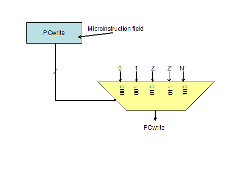
By using 000 we can set PCwrite=0, with 001 we can set PCwrite=1, with 010 we get PCwrite=Z, and so on. We could add more inputs to the MUX for supporting other conditions for PC. Alternatively we could use the nextPC selection field to allow PCwrite to take different values depending on Z and N.
Let us now discuss the next microPC selection field. If you look at the FSM for the multicycle control you will notice two types of transitions:
- Transitions that are independent of any datapath state such as the transition from cycle 1 to cycle 2, or from cycle 3 to cycle 4 for the ADD instruction.
- Transitions that dependent on datapath state. Specifically the next state after cycle 2 depends on the value of bits 3…0 of the IR. This is the instruction opcode.
We can design the next microPC selection field so that it supports both types. Here’s one possibility:
|
Type |
Next microPC |
“Type” will be a single bit. 0 means direct, in which case the next microPC field is written directly in the microPC. This allows direct transitions from state A to state B that are independent of datapath state. When Type=1 microPC is updated as follows: microPC=microPC + Inst3…0 + next microPC. So, for example assuming that type=1 and nextmicroPC=1, then for a LOAD instruction we will have microPC=microPC + 0000 + 1. For an ADD we will have microPC=microPC + 0100 + 1.
A complete microprogram implementing the FSM of the multicycle implementation follows. The microinstruction at address 1 uses the INST3…0 field to determine which is the next microinstruction to execute, so the next microPC becomes 1 + Inst3…0 + 1. The following table lists all possibilities based on the Inst3…0 value:
|
Inst3…0 |
1 + inst3…0 + 1 |
Instruction |
|
0000 |
2 |
LOAD |
|
0001 |
3 |
None |
|
0010 |
4 |
STORE |
|
0011 |
5 |
SHIFT X010 |
|
0100 |
6 |
ADD |
|
0101 |
7 |
BZ |
|
0110 |
8 |
SUB |
|
0111 |
9 |
ORI X111 |
|
1000 |
10 |
NAND |
|
1001 |
11 |
BNZ |
|
1010 |
12 |
None |
|
1011 |
13 |
SHIFT X011 |
|
1100 |
14 |
None |
|
1101 |
15 |
BPZ |
|
1110 |
17 |
None |
|
1111 |
17 |
ORI X111 |
Notice that some possibilities do not correspond to instructions we have defined. For example there is no instruction that has 0001 in INST3…0. In addition, ORI and SHIFT map to more than two possibilities since they only use three of the four INST bits.
|
address / comment |
Datapath control signal values |
Next microPC selection |
|
||||||||||||||||
|
|
PCwrite |
AddrSel |
MemRead |
MemWrite |
IRload |
R1Sel |
MDRload |
R1R2load |
ALU1 |
ALU2 |
ALUop |
RFWrite |
RegIn |
ALUOutWrite |
FlagWrite |
Type |
Next microPC |
||
|
0 / cycle 1 |
001 |
1 |
1 |
0 |
1 |
0 |
0 |
0 |
0 |
001 |
000 |
0 |
0 |
0 |
0 |
0 |
00000001 |
||
|
00000001 / cycle 2 next microPC = microPC + Inst3…0, so next microPC can take any value from 2 through 17 |
000 |
0 |
0 |
0 |
0 |
0 |
0 |
1 |
0 |
000 |
000 |
0 |
0 |
0 |
0 |
1 |
0 |
||
|
2 / cycle 3 LOAD |
000 |
0 |
1 |
0 |
0 |
0 |
1 |
0 |
1 |
000 |
000 |
0 |
0 |
0 |
0 |
0 |
18 |
||
|
3 / no instruction / reserved for future expansion |
|
|
|
|
|
|
|
|
|
|
|
|
|
|
|
|
|
||
|
4 / cycle 3 STORE |
000 |
0 |
0 |
1 |
0 |
0 |
0 |
0 |
1 |
000 |
000 |
0 |
0 |
0 |
0 |
0 |
0 |
||
|
5 / cycle 3 SHIFT |
000 |
0 |
0 |
0 |
0 |
0 |
0 |
0 |
1 |
100 |
100 |
0 |
0 |
1 |
1 |
0 |
19 |
||
|
6 / cycle 3 ADD |
000 |
0 |
0 |
0 |
0 |
0 |
0 |
0 |
1 |
000 |
000 |
0 |
0 |
1 |
1 |
0 |
19 |
||
|
7 / cycle 3 BZ |
010 |
0 |
0 |
0 |
0 |
0 |
0 |
0 |
0 |
000 |
000 |
0 |
0 |
0 |
0 |
0 |
0 |
||
|
8 / cycle 3 SUB |
000 |
0 |
0 |
0 |
0 |
0 |
0 |
0 |
1 |
000 |
001 |
0 |
0 |
1 |
1 |
0 |
19 |
||
|
9 / cycle 3 ORI |
000 |
0 |
0 |
0 |
0 |
1 |
0 |
1 |
0 |
000 |
000 |
0 |
0 |
0 |
0 |
0 |
20 |
||
|
10 / cycle 3 NAND |
000 |
0 |
0 |
0 |
0 |
0 |
0 |
0 |
1 |
000 |
011 |
0 |
0 |
1 |
1 |
0 |
19 |
||
|
11 / cycle 3 BNZ |
011 |
0 |
0 |
0 |
0 |
0 |
0 |
0 |
0 |
000 |
000 |
0 |
0 |
0 |
0 |
0 |
0 |
||
|
12/ no instruction / reserved for future expansion |
|
|
|
|
|
|
|
|
|
|
|
|
|
|
|
|
|
||
|
13 / cycle 3 SHIFT |
000 |
0 |
0 |
0 |
0 |
0 |
0 |
0 |
1 |
100 |
100 |
0 |
0 |
1 |
1 |
0 |
19 |
||
|
14 / no instruction / reserved for future expansion |
|
|
|
|
|
|
|
|
|
|
|
|
|
|
|
|
|
||
|
15 / cycle 3 BPZ |
100 |
0 |
0 |
0 |
0 |
0 |
0 |
0 |
0 |
000 |
000 |
0 |
0 |
0 |
0 |
0 |
0 |
||
|
16 / no instruction / reserved for future expansion |
|
|
|
|
|
|
|
|
|
|
|
|
|
|
|
|
|
||
|
17 / cycle 3 ORI |
000 |
0 |
0 |
0 |
0 |
1 |
0 |
1 |
0 |
000 |
000 |
0 |
0 |
0 |
0 |
0 |
20 |
||
|
18 / cycle 4 LOAD |
000 |
0 |
0 |
0 |
0 |
0 |
0 |
0 |
0 |
000 |
000 |
1 |
1 |
0 |
0 |
0 |
0 |
||
|
19 / cycle 4 ALU |
000 |
0 |
0 |
0 |
0 |
0 |
0 |
0 |
0 |
000 |
000 |
1 |
0 |
0 |
0 |
0 |
0 |
||
|
20 / cycle 4 ORI |
000 |
0 |
0 |
0 |
0 |
0 |
0 |
0 |
1 |
011 |
010 |
0 |
0 |
1 |
1 |
0 |
21 |
||
|
21 / cycle 5 ORI |
000 |
0 |
0 |
0 |
0 |
1 |
0 |
0 |
0 |
000 |
000 |
1 |
0 |
0 |
0 |
0 |
0 |
||
Let’s see how ORI 7 would be executed using this microprogram. Initially, microPC=0. Note that ORI 7 is encoded as 0011 1111
Cycle 1:
microPC=0
the
microinstruction sets PC=PC+1, IR=Mem[PC] and microPC=1
Cycle 2:
microPC=1
The microinstruction does R1=RF[IR7..6], R2=RF[IR5…4] and microPC=1 + IR3…0 + 1 = 1 + %1111 + 1 = 17
Cycle 3:
microPC=17
The microinstruction does R1=RF[1] and microPC=20
Cycle 4:
microPC=20
The microinstruction does ALUOut=R1 OR ZE(Imm5), Z&N updated, and microPC=21
Cycle 5:
microPC=21
The microinstruction does RF[1] =AluOut and microPC=0.
Note that the FSM we implemented is slightly different than then one we implement previously. The difference is that ADD, SUB and NAND use separate states. This is necessary since in the new design we cannot have ALUop be a function of IR3…0. So, we can’t have them share states where ALUop=ADD/SUB/NAND depending on IR3…0.