Interfacing with Slower Memories
Andreas Moshovos
Spring 2007
In the implementation we have described thus far we assumed that memory took a single cycle to respond. However, the larger the memory the slower it is. Instead of making our CPU cycle long enough to accommodate slower memories what we can do instead is change the control so that it allows for multiple cycles while interacting with memory. In this lecture we will discuss different ways of implementing this functionality. The first will use extra wait states. The second, will decouple the wait state functionality into a separate small FSM. The two aforementioned implementations will still assume that the number of cycles required by memory is known at design time. The last implementation will allow memory to delay the CPU as long as it is necessary.
Hardwired Wait States
The simplest implementation is to introduce additional “wait” states every time we access memory. For example, if we knew that memory requires 3 cycles to respond to our requests what we could change our FSM so that it takes three cycles to perform a memory operation. The following diagram shows how the “cycle 1” to “cycle 2” state transition would change to accommodate the slower memory. Similar changes are needed for Cycle 3 for LOAD and STORE.
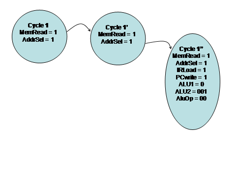
The states “cycle 1” and “cycle 1’” are used to wait for memory to respond to our read request. Notice that in these two states we keep MemRead = 1 and the Address steady using the PC’s output.
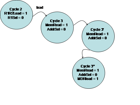
Here are the additional changes for the LOAD instruction:
And the changes for the STORE instruction:
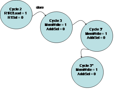
In both cases we are steadily driving the memory address lines using R2’s output (AddrSel = 0) and setting corresponding MemRead or MemWrite to 1.
The nuisance with the implementation we described is that any time the relative timing of memory to CPU changes we need to redesign the control to introduce additional or remove wait states. The relative latency of memory compared to the CPU may change either because we change the memory device or because we change the CPU.
Decoupling the
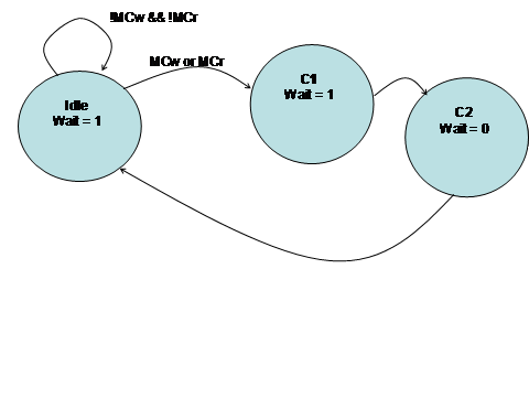
Instead of introducing new states every time we need to access memory we can delegate this functionality to a separate, dedicated FSM. The FSM would accept inputs from the main control FSM and provide an output that will be used by the main FSM to wait at a stage. Let us use the term memory controller or MC for this small FSM. The MC has two inputs MCr and MCw which respectively initiate a memory read and a memory write. MC produces a single output wait which is 1 while t.
Here’s the state transition diagram for MC assuming that memory takes 3 cycles to complete a request:
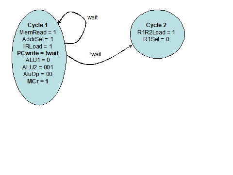
Here’s how the main control FSM has to change. Here’s the transition from cycle 1 to cycle 2:
Here’s how the MC delays the main FSM for three cycles:
Cycle 1
In the state “cycle 1” the main FSM initiates a memory read and notifies the MC with MCr=1. The MC is in its idle state, so wait is 1. Accordingly, the main FSM remains at “cycle 1”. Notice that while we are calculating PC+1, we do not write it into the PC since PC=!wait. We will allow the write to happen only when the MC signals that the operation has completed. At the end of cycle 1, the main FSM will remain in state “cycle 1” while the MC will move to state “C1”.
Cycle 2
The main FSM remains at state “cycle 1”. At the end the MC will move to state “C2” where wait will become 0.
Cycle 3
The main FSM will move to state “cycle 2” at the end of this cycle. Because wait is 0, PCwrite becomes 1 and at the end of the cycle PC will become PC + 1.
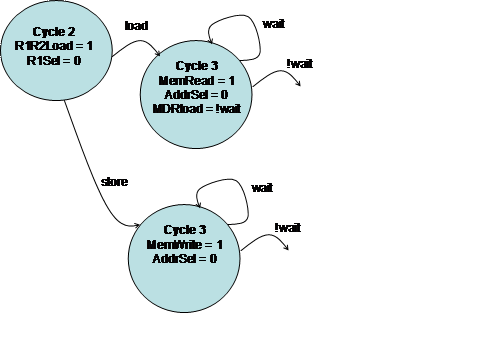
Here are the changes for the LOAD and STORE instructions:
If we wanted to use a slower memory that requires say 5 cycles to respond then we only need to change the MC FSM. The main FSM remains the same.
External Wait signal
The final implementation allows memory to delay the main FSM as long as it is necessary. Instead of using a MC FSM, we instead allow memory to set the wait signal. If memory is as fast as the CPU, wait must be tied to 0 so that the main FSM never stalls at a state. If memory is slower than the CPU, then normally wait should be at 1. An external controller will have to set wait 0 only when memory becomes ready and only for one cycle.
Synchronous vs.
Asynchronous Memory Interfaces
The last implementation can be used with both a synchronous and an asynchronous memory interface. A memory interface is synchronous if it uses the same clock as the CPU and times its responses accordingly. In a synchronous interface signals change sufficiently before the next clock edge (negative in our examples) so that the CPU will observe steady values at the clock edge. In an asynchronous interface, memory does not time its responses according to the CPU clock. Accordingly, care must be taken to avoid a scenario where memory is still producing its output while a clock edge occurs. Since the memory outputs can be in an intermediate state, the CPU will be reading a “random” value. In subsequent courses you will see methods for avoiding this scenario.