Bus-Based Implementation
Andreas Moshovos
Spring 2007
In this lecture we will describe a different implementation style. We will use the term bus-based implementation. We will first describe the datapath and then provide RTL (register transfer language) for some of the control states. This is a multi-cycle implementation. The key difference is that we do not design a datapath with point-to-point connections amongst the various units. Instead we assume a common bus and connect all inputs and outputs of all units to that bus. We are going to use the same building blocks (e.g., Register File and ALU). The following figure shows for example how the PC will be connected to the common bus:
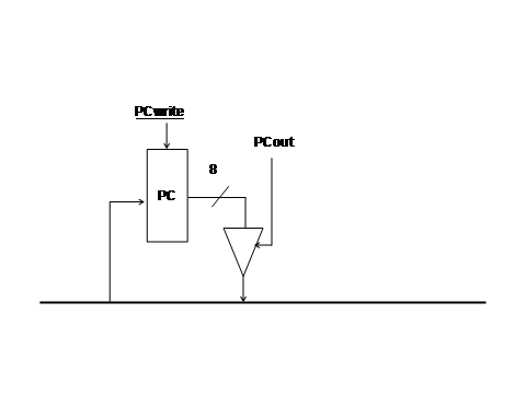
As you see in the figure, the PC input is directly connected to the common bus and the PC’s output is also connected to the common bus via a tri-state buffer. The PCout signal controls the tri-state buffer. If PCout is 0, the PC does not place a value on the bus. If PCout is 1, the PC places its value on the bus. All outputs will be connected in this manner with the common bus. At any given point of time at most one output should be activated.
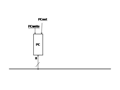
For clarity we will not show the detailed connections. Instead we will use the following diagram:
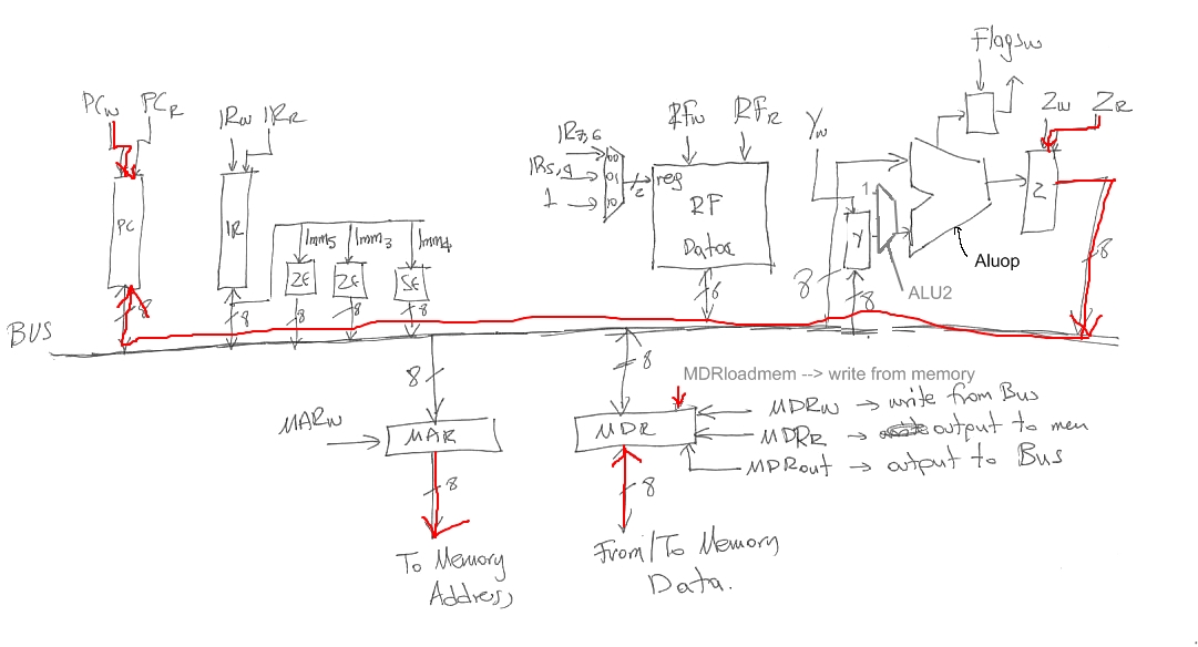
Here’s the complete datapath:
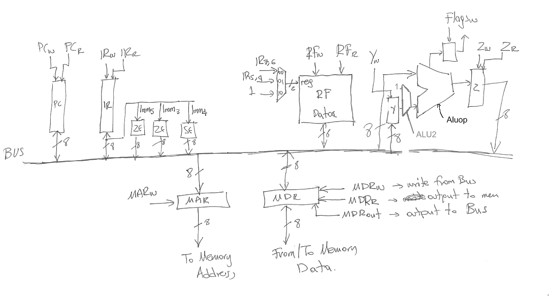
Notice that the register file has a single port that can be used to either read or write one register at a time. All input data ports are connected to the BUS and all output dataports are again connected via tri-state buffers. With this arrangement we can copy a value from one element (e.g., the PC) to another (e.g., the second input of the ALU). The memory interface contains two registers. One for addresses (MAR) and one for data (MDR). Also notice that there are two temporary registers associated with the ALU. One is connected to the second input (Y) and the other (Z) is connected to the ALU’s output.
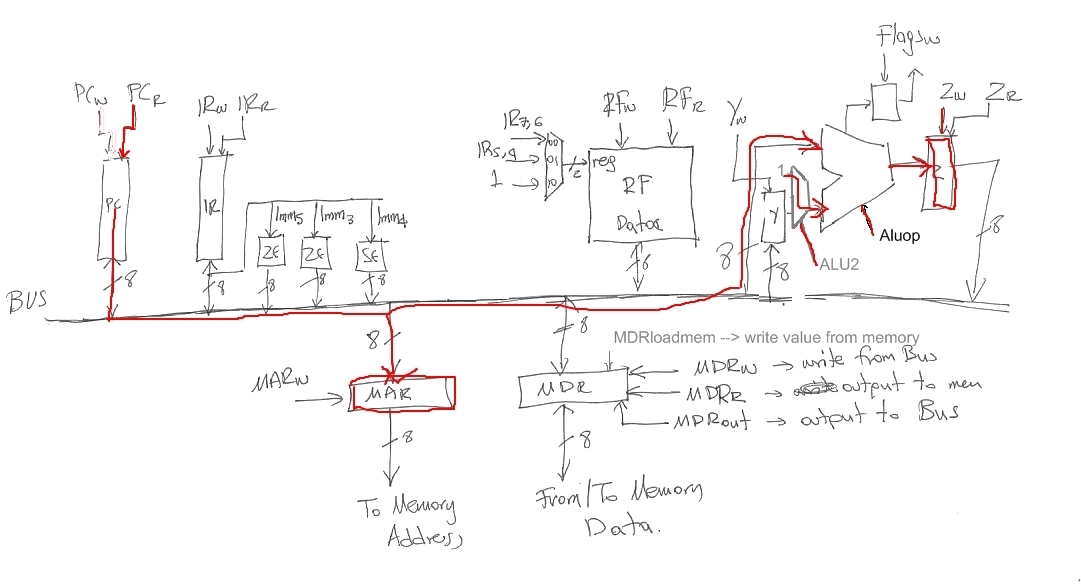
Let’s see how we can implement the equivalent of “cycle 1” from our previous multi-cycle implementation. Here are the control signals that must be asserted:
CYCLE 1: PCr, MARw, MemRead, ALU2=0, ALUop=ADD, Zw
PCr places the PC’s value on the bus. MARw loads the value from the bus, i.e., the PC, into the memory address register. MemRead initiates a memory read, ALU2=0 selects 1 as the second input to the ALU, the ALU calculates BUS value + 1 and since BUS value=PC it calculates PC + 1. Zw stores the value calculated by the ALU into the Z register:
In Cycle 2 we wait for the value from memory and also write the value PC+1 from the Z register back to the PC:
Zr, PCw, MDRloadmem=!wait
Where the wait signal is generated by the memory controller as we described in a previous lecture.
Note: The book uses “wait for memory controller” or WFMC instead of MDRloadmem=!wait.
Here’s what happens in the datapath:
Finally in cycle 3 we can copy the value read from memory into IR:
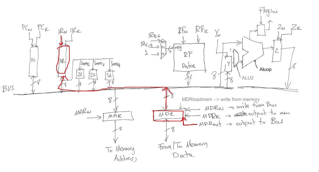
From cycle 4 onwards the control can differentiate based on the instruction. Accordingly the actions will be different.
Here’s how we execute an ADD instruction:
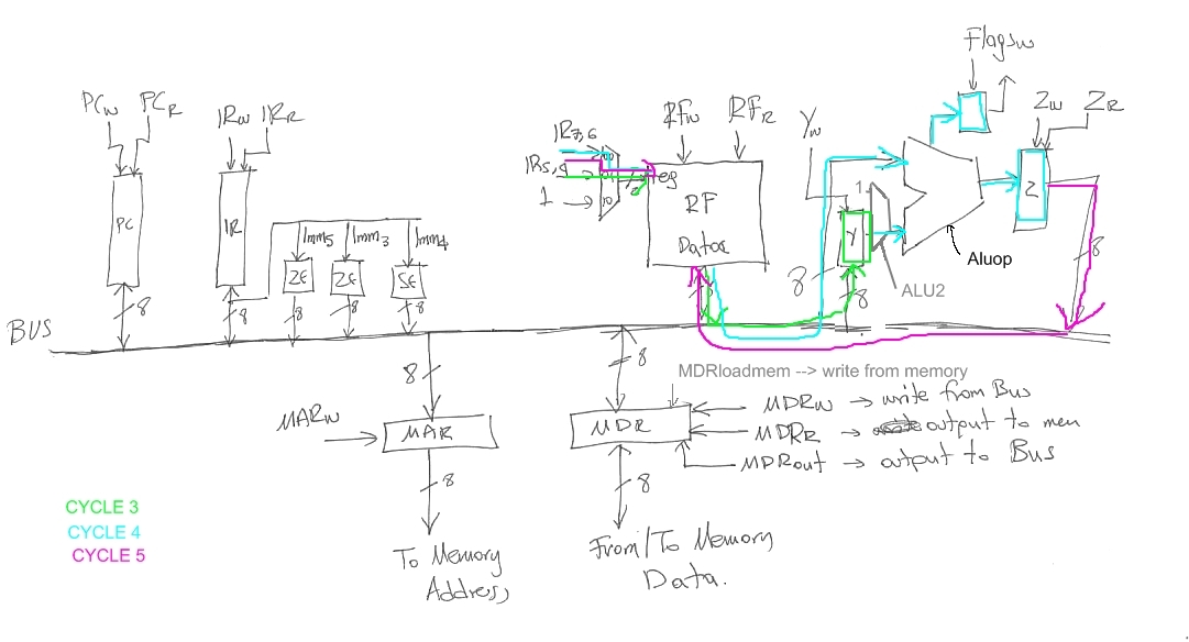
In cycle 3 we read register using the R2 field from IR and write its value into the temporary register Y.
In cycle 4 we read a register using the R1 field from IR, add the register value and Y using the ALU, and write the sum into the Z register also updating the flags.
In cycle 5, we write the value from the Z register back to the register file using the R1 field as the register name.
Here’s how a LOAD would execute:
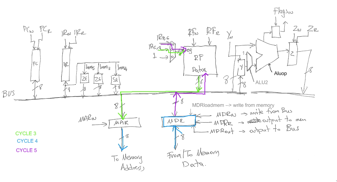
In Cycle 3 we read a register using the R2 field from the IR and write that value into MAR. At the end of the cycle we initiate a memory read.
In cycle 4, we wait for memory to respond and write the memory value into MDR.
In cycle 5, we copy the MDR value into the register file using the R1 IR field to identify the register.
The book describes this steps as follows:
Cycle 3: Rsel=01, MARw, MemRead
Cycle 4: WFMC, MDRloadmem
Cycle 5: MDRout, RFw, Rsel=00
Where Rsel is the signal that controls the mux on the input of the RF (not shown on the diagram).