ECE243
Spring 2008
Andreas Moshovos
Attaching Devices
to the Processor’s Memory Interface
In this lecture we will discuss an implementation of the parallel interface (PIT) and how it can be connected to the processor’s memory interface. Recall that all devices in NIOS II are memory mapped. That is, they appear as part of the memory address space and the processor can access them using regular loads and stores.
Recall that the PIT interface presents a programming interface that consists of two bytes in memory. For port JP1A the two registers are:
1. The DATA register (DR) at address 0x00FF1110
2. The DIRECTION register (DIR) at address 0x00FF1110+4 = 0x00FF1114
|
Address |
BYTE |
|
|
0x00FF1110 |
DR |
Data Register |
|
|
Unused |
|
|
|
Unused |
|
|
|
Unused |
|
|
0x00FF1114 |
DIR |
Direction Register |
|
|
Unused |
|
|
|
Unused |
|
|
|
Unused |
|
The PIT provides eight connections to the outside world that can be configured, independently to act as inputs or outputs. The direction of each connection is controlled by the DIR. The DIR has 8 bits each corresponding to one of the outside connections. Setting a DIR bit to 1 makes the connection an output, i.e., the NIOS II sets the value, while setting a DIR bit to 0 makes the connection an input, i.e., an outside source is supposed to set a value which can be read by NIOS II. The DR register can be used to either read or set the values on the connections.
Let us review how the programmer accesses the PIT. The following example code, sets the upper four bits as outputs, then reads the value of all eight connections and finally sets the upper four bits to 1:
movia r8, 0xFF1110
movi r9, 0xF0
stwio r9, 4(r8) # set the upper four connection to be outputs
ldwio r10, 0(r8) # read the values on the PIT connections
stwio r9, 0(r8) # set the upper four connections to 1
In time, NIOS II will perform first a memory write at address 0xFF1114 writing the value 0xF0, then a memory read from address 0xFF1110, and finally a memory write at address 0xFF1110 writing again the value 0xF0. The PIT will have to respond to all these requests.
Having seen how to program the PIT we can now discuss an implementation. This is not necessarily how it is implemented on the DE2. At the physical level the PIT presents the following signals:
1. Data: a set of 8 wires that are used for supplying the value to written to registers DIR or DR, or to read the value from the DR. These signals can be used as input or as output as explained subsequently.
2. A DIR write signal: When this is 1 the value in the Data is written into the DDR
3. A DIR write signal: When this is 1 the value in the Data is written into the DR
4.
5.
What appears to software as a single register DR is implemented using separate elements for input and output. The DRO latch implements the output portion, while a tri-state buffer is used for the input portion. Here’s the diagram of one PIT bit:
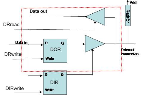
The DRO and DIR boxes are latches. The DRO implements the output portion of the DR register, while DIR implements the DIR register. We can change their value using the Data (D) and Write signals. The DIR latch output drives a tri-state driver whose output is connected to the external connection. If DIR is 1 then the tri-state buffer behaves like a buffer and passes the value of the DOR latch to the external connection. If DIR is 0 then the tri-state buffer is placed in the off state which can be thought as an open switch (no connection). In this case, an external source will determine what the value is on the external connection wire. The resistor is there to help when DRO wants to drive a 1 (high voltage) since the technology used is not very “strong” when driving a one. The registor also sets the external connection to 1 when no one is driving it.
The DR register is implemented by the elements shown inside the red-dotted box. If DRread becomes 1 then the upper tri-state buffer is activated and passes the value on the external connection to the data_out wire. If DRwrite becomes 1, then the value provided on the data_in wire is written in the DOR bit. Provided that the DIR bit is also 1 this value appears on the external connection.
What we have described is just one of the 8 slices used by the PIT. The 8 slices are connected together so that they share the Write and Read lines and so that their data lines collectively form the 8-bit data interface of the PIT.
Connecting the PIT
to the NIOS II Memory Interface
Let’s us now discuss how we can connect the PIT to the NIOS II processor’s memory interface. Here’s the interface as we discussed it in the previous lecture:
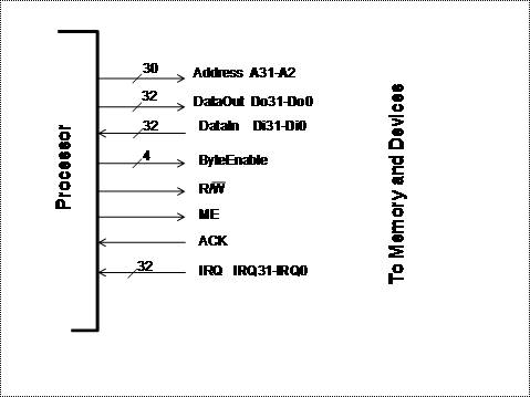
To connect the PIT to the memory interface described previously, we first connect the PIT data_in and data_out lines to the lower byte (8 bits) of the NIOS II data_out and data_in respectively. This will allow us to access the three PIT elements (DIR, DR for write and DR for read) by using load and store memory accesses. Then we need to activate the corresponding PIT elements depending on the address accessed.
We need to detect the following combinations on the address lines: 0xFF1110 for read and write from/to the DR, and 0xFF1114 for write only (writes to DIR).
Here are the functions we need to implement:
DIRwrite = (address == 0xFF1114) and (R/!W == 0) and (ByteEnable0 == 1) and (ME == 1)
DRread =(address == 0xFF1110) and (R/!W == 1) and (ByteEnable0 == 1) and (ME == 1)
DRwrite =(address == 0xFF1110) and (R/!W == 0) and (ByteEnable0 == 1) and (ME == 1)
We break these problems into two sub-problems: first detect the address on the address lines, and then detect whether the processor requests a read or a write.
Detecting the
Address
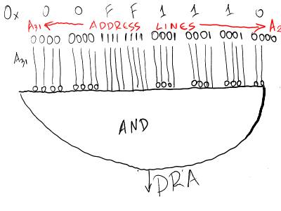
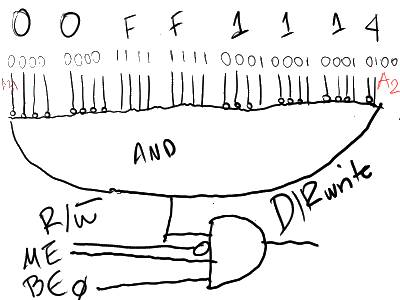
This process is called address decoding. In the simplest to describe implementation we use a 30 input AND gate for detecting the addresses. We only need a 30-input AND gate since NIOS II omits the 2 least significant bits of addresses (it uses the ByteEnable signals in their place). Let’s see how we decode the address 0x00FF1110. Using a 30-bit input here’s how we can detect this combination on the address lines: write the number in binary. For every digit that is 1 connect the corresponding wire directly to the AND gate. For every digit that is 0, connect the corresponding wire first to inverter and then connect the output of the inverted to the AND gate.
Here’s the ADDRESS DECODING part for DR, it generate the signal DRenable that tells us that the processor is either reading or writing DR:
The DRA signal can now be combined with R/!W, ByteEnable0, and ME to generate the DRread and DRwrite signals:
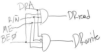
Here’s the address decoding and signal generation circuit for DIRwrite:
In total we used two 30-input AND gates, three 4-input AND gates, plus two NOT gates (actually, one is sufficient since both invert R/!W). Each of the two 30-input AND gates is connected to all 30 address signals. By using inverters appropriately we can detect that the address being accessed is one of those mapped to DR, and DIR. We start by looking at the binary representation of these addresses and put an inverter for those address bits that are zero in the pattern we are interested in. After detecting the address, we then used a 4-input AND gate to detect accordingly whether an access is being made (ME == 1 – ME is Master Enable), whether it is a read or a write, and whether the least significant byte of the interface is activated.
This implementation is easy to understand, however, it’s not necessarily the most efficient. This topic is beyond the scope of this lecture, however, you are encouraged to think of ways of reducing the number of components needed to do address decoding.
Here’s the complete design:
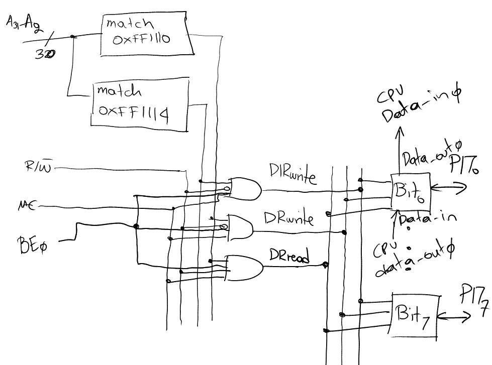
Each
bit cell (there are eight of them) is as shown earlier). The boxes labeled
“match some hex value” are the 32-bit input AND gates we described earlier.
Generating the ACK
signal
As described the NIOS II memory interface requires that
the device generates an ACK signal when the request is completed. In out PIT
design this is straightforward if we assume that the response is ready in a single
cycle. The ACK signal can then be the OR of DRwrite, DRread, or DIRwrite. Here’s the
circuit for it:
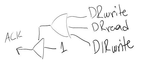
Note that we did not drive the ACK signal directly. We instead used a tri-state buffer to selectively drive a 1 on it. This is because the ACK signal is shared by all devices and memory. So there are many potential sources for this signal. At any given point of time at most one device should be driving this signal. By using a tri-state buffer at each connection we make sure that each device either drives the ACK to 1, or leaves the ACK line floating to be set by another device.