The Processor’s
Interface to Memory and Devices
Spring 2008
Andreas Moshovos
In this lecture we will discuss the physical interface of the processor to memory and devices. In previous lectures we have seen the programmer’s view of memory and devices. Here we’ll see an example of how the necessary support is implemented in hardware. We will then explain how memory and other devices can be connected to this interface. Typically, you’ll see the term “external bus” used to refer to the processor’s interface. This is appropriate most of the time since most systems do indeed use a bus for the external interface. A bus is physically a set of wires that is connected to all devices directly. Modern high-performance systems may use a different physical interface that relies on point-to-point connections instead, however, conceptually, these interfaces are similar.
We will describe an interface for the NIOS II processor. NIOS II is a soft processor so this is not the only possible interface, however, what we describe is representative of other interfaces and of that provided by the NIOS II vendor. Since devices are memory mapped, the same physical interface is used by both. The interface needs to support loads and stores, that is memory reads and writes. The interface we are describing also supports different datatypes: it supports reads and writes of a byte, two bytes or four bytes (corresponding to the byte, half-word and word datatypes of NIOS II). Recall that the interface is that of memory. Hence it needs to support LOADS and STORES.
Here’s the physical interface:
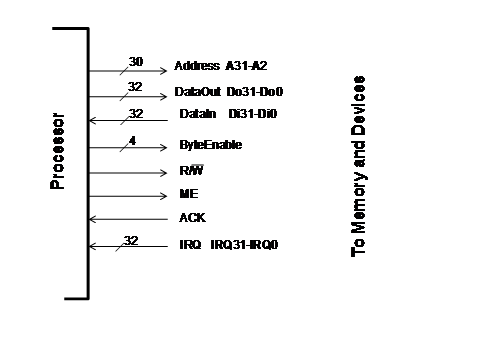
Here’s what the various signals do:
|
Signal |
Acronym |
Width |
Type |
Function |
|
Address |
A31-A2 |
30 |
Output |
Specifies a word address to access Using the ByteEnable signals we can access any combination of the four bytes within the word. More on this later. |
|
DataOut |
Do31-Do0 |
32 |
Output |
Contain the data when performing a write, only those bytes that are enabled via ByteEnable are valid |
|
DataIn |
Di31-Di0 |
32 |
Input |
Contain the data when performing a read, only those bytes that are enabled via ByteEnable are expected to be valid |
|
ByteEnable |
BE0-BE3 |
4 |
Output |
Specify which bytes within the word are to be accessed. More on this later. |
|
Read/!Write |
R/!W |
1 |
Output |
1 means do a read, 0 means do a write |
|
Master Enable |
ME |
1 |
Output |
1 means all other outputs are valid, 0 means ignore all other signals |
|
Acknowledge |
ACK |
1 |
Input |
Normally this is 0. The device/memory that is accessed is supposed to set this to 1 once it has completed the request. That is, once it has written the data for writes, or once it has placed the right data on Di for reads. |
|
Interrupt Request |
IRQ31-IRQ0 |
32 |
Input |
Interrupt Request signals. A device sets this to 1 to request an interrupt. |
Here’s the sequence of actions that take place to perform a read (load). Initially, MasterEnable is 0 indicating that no action is taking place. At this point ACK is also 0. Then the following happens in order:
READ/LOAD
SEQUENCE:
Processor:
1. Prepare all necessary by setting them to the appropriate values. The signals that must be set are:
a. Address
b. ByteEnable (for the time being please ignore how these are set, we will discuss this shortly).
c. R/!W
2. Set ME to 1
Device or Memory
3. Access the specified bytes and place them on the DataIn lines
4. Set ACK to 1
Processor
5. Read data of the DataIn lines
6. Set ME 0 (note that the NIOS II interface de-asserts this ealier – more on this later)
Device or Memory
7. Set ACK to 0
WRITE/STORE
SEQUENCE:
Processor:
8. Prepare all necessary by setting them to the appropriate values. The signals that must be set are:
a. Address
b. DataOut
c. ByteEnable (for the time being please ignore how these are set, we will discuss this shortly).
d. R/!W
9. Set ME to 1
Device or Memory
10.Update the specified memory locations with the values given on DataOut
11.Set ACK to 1
Processor
12.Set ME 0 (note that the NIOS II interface de-asserts this ealier – more on this later)
Device or Memory
13.Set ACK to 0
Notice that at the end, as with reads, we are back to the initial state of ME = 0 and ACK = 0.
The ByteEnable Signals and the Use of 30-bit Addresses
Our interface is capable of transferring up to 32 bits per access. However, not all NIOS II accesses are 32-bit wide. In particular, Because NIOS II supports byte and half-word accesses in addition to word accesses. To support these we use the ByteEnable signals and only the upper 30 bits of the address accessed. All addresses on our interface are word-aligned. That is, the two least-significant bits that are omitted are implied to be 0. There are four bytes within each word. Each ByteEnable line corresponds to one of these bytes. BE0 corresponds to the byte that is at the same address the word starts, while BE3 is 3 bytes after that. Here are a couple of examples to clarify things. All numbers are in binary
|
Operation |
A31-A2 |
BE3-BE0 |
Di31-Di0 |
Explanation |
|
LOAD.WORD 10000 |
0…0100 |
1111 |
All must be set by memory |
Access four bytes starting from address 10000 |
|
LOAD.HWORD 10000 |
0…0100 |
0011 |
Di0-Di15 must be set by memory |
Access two bytes starting from address 10000 |
|
LOAD.HWORD 10010 |
0…0100 |
1100 |
Di31-Di16 must be set by memory |
Access two bytes starting from address 10010 |
|
LOAD.BYTE 10000 |
0…0100 |
0001 |
Di0-Di7 must be set by memory |
Access the byte at address 10000 |
|
LOAD.BYTE 10001 |
0…0100 |
0010 |
Di15-Di8 must be set by memory |
Access the byte at address 10001 |
|
LOAD.BYTE 10010 |
0…0100 |
0100 |
Di23-Di16 must be set by memory |
Access the byte at address 10010 |
|
LOAD.BYTE 10011 |
0…0100 |
1000 |
Di31-Di24 must be set by memory |
Access the byte at address 10001 |
|
LOAD.BYTE 11010 |
0…0110 |
0100 |
Di23-Di16 must be set by memory |
Access the byte at address 11010 |
|
LOAD.BYTE 11101 |
0…0111 |
0010 |
Di15-Di8 must be set by memory |
Access the byte at address 11101 |
The Role of the
Master Enable Signal
Besides being able to say to memory “do noting” ME plays another important role. In the physical world it takes time for us to setup coherent values on all signals. For example, assume we want to perform in sequence a STORE.BYTE 0x10, 0X000000 and a STORE.BYTE 0x01, 0xffffff. It is practically impossible to change all signals instantaneously. So, in going from address 0x000000 to 0xffffff all possible binary numbers may temporarily appear (because different signals may change at different rates). Without the ME, the memory could get confused and misinterpret the second store. With ME, we can se ME to zero in between the two stores, wait sufficient time for the second store values to appear on the data and address signals and then set ME=1. This way memory remains oblivious to temporarily inconsistent values.
The Role of the
Acknowledge Signal
Memory devices and I/O devices can have different latencies. To allow an device to delay the processor as long as it is necessary the NIOS II designers included the ACK signal. A device keeps ACK to 0 while it is performing the requested operation. It then sets ACK to 1 to notify the processor that the request was completed. Because this is a device generated signal different devices can delay the processor by a different amounts of time. For example, if all devices are as fast as the processor’s interface is, then we can simply connect ACK to ME. This way all requests are acknowledged immediately.
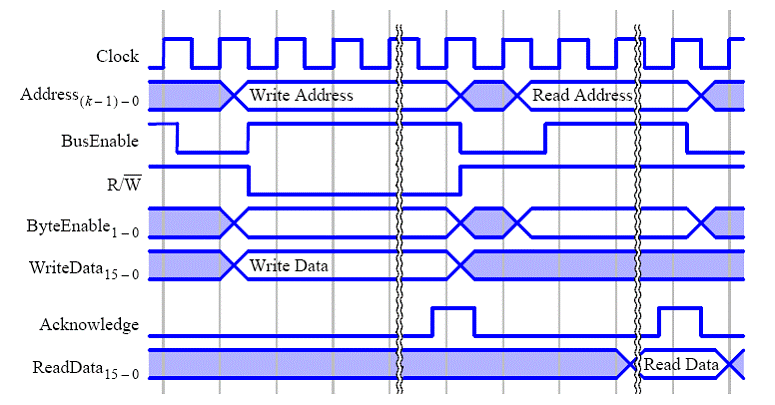
Synchronous vs.
Asynchronous Interfaces
The NIOS II interface is synchronous. That is, in addition to the signals shown, an extra clock signal is provided by the processor. All signals are sampled on the rising edge of this clock. Here are timing diagrams for memory reads and writes (note that in this diagram BusEnable = MasterEnable, WriteData=Do, and ReadData=Di):
This is not true:
The NIOS II designers optimized for speed by asserting MasterEnable
only at the beginning of each request and only for one cycle. This way, the
processor does not need to de-assert MasterEnable after the device responds with an ACK.
So, here are the actual read and write sequences:
READ/LOAD
SEQUENCE:
Processor:
1. Prepare all necessary by setting them to the appropriate values. The signals that must be set are:
a. Address
b. ByteEnable (for the time being please ignore how these are set, we will discuss this shortly).
c. R/!W
2.
Set ME to 1
Device or Memory
3. Access the specified bytes and place them on the DataIn lines
4. Set ACK to 1 for one cycle
Processor
5. Read data of the DataIn lines. This happens on the rising edge when ACK is 1
6.
Set ME to 0
WRITE/STORE
SEQUENCE:
Processor:
7. Prepare all necessary by setting them to the appropriate values. The signals that must be set are:
a. Address
b. DataOut
c. ByteEnable (for the time being please ignore how these are set, we will discuss this shortly).
d. R/!W
8.
Set ME to 1
Device or Memory
9. Update the specified memory locations with the values given on DataOut
10.Set ACK to 1
11.Set
ME to 0
The original sequences we described can be used without a clock. Such an interface is asynchronous as it does not use a clock.
The NIOS II interface can support only one outstanding request at any given point in time. This is appropriate for the target application since NIOS II is not a high-performance design. In modern high-performance systems, however, memory and devices are typically a lot slower than the processor and its interface (the interface typically runs only at a fraction of the CPU’s clock). Reserving the interface for the duration of a single request results in low utilization. If the processor is capable of performing multiple operations, we can instead use a split-transaction interface. There, the processor initiates a request by providing the appropriate information (e.g., address, byteenable, r/w and data if necessary) and the devices copies this information locally. The interfaces is then used to initiate other requests. Eventually, when the device is ready to respond, it sends the response back to the processor. Each request is tagged so that it can be matched with its response. Further details on this concept are beyond the scope of this course.
Multiplexing data_in
and data_out
In our preceding design
two separate sets of 32 wires each were used for reading and for writing data
from and to memory respectively. Often times, the number of pins available per
chip is limited by cost (a integrated circuit becomes
increasingly and significantly more expensive the more pins it uses).
Accordingly, designers often try to find ways to reduce the number of external
connections (pins). In our memory we could “multiplex”
the data_in and data_out
signals. This does not violate the behavioral model as it does not support
simultaneous reads and writes. We can only read or write but not both at the
same time.
One way of multiplexing these wires is via the
use of tri-state buffers. The symbol/connections for a tri-state buffer and its
truth table are as follows:
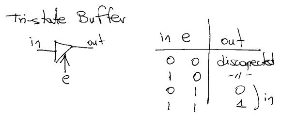
When the e input is zero the in and out
terminals are as if they are completely disconnected. Using 32 tri-state
buffers one per data bit we can multiplex the data_in
and data_out signals as follows:
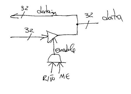
Only when we do a read (R/W’ = 1 and ME = 1), the tri-state buffers are enabled and memory
“drives” (i.e., places a value) on the data wires. In all other cases, the data
wires behave as inputs so they can be freely set to any value desired (i.e.,
when doing a write).
Using this methodology we can build a bus where
multiple devices are connected to the same set of wires and by appropriately
enabling their outputs we can make sure that only one device is “driving”
(i.e., placing a value) on the bus and others (one or many) are reading it. As
a side-note, please keep in mind that these busses do not scale very well
primarily as a result of increased parasitic
capacitance on the wires.
Multiple Master
Interfaces
The NIOS II interface has only one “master”, that is a party that can initiate requests. That is the processor. For higher performance, most modern systems implement an interface that can support multiple masters. In such an interface additional signals are provided so that some other party (e.g., an I/O device such as a disk controller) can temporarily become the bus master. This allows devices to communicate amongst them and with memory without processor intervention. In such an interface the address and DataOut lines are not always driven by the processor. The processor uses tri-state connections to them so that other devices can drive values on them as needed. Extra signals are provided so that a device can request to become a master, and to relinquish control back to the processor.