Professor Paul Chow and Professor Jonathan Rose
Fall 1996
**** need to get the datasheet for the 74193
The goals of this lab are to understand the operation of JK flip flops, counters, and ring oscillators. These components are used to build an experiment to measure the delay of a gate.
Note: When building this circuit, you will have some unused inputs. What can happen if you leave them floating (unconnected)? What is the solution?
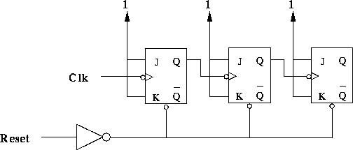
Figure 1: A 3-bit ripple counter.
Do not disassemble this circuit. You will need it for PART II.
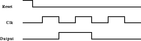
Figure 2: Timing of the desired output.
The circuit shown in Figure 3 consists of three inverting gates
connected in a ring. While the Enable input is equal to 0, points
![]() , and
, and ![]() will be at logic levels 1, 0
and 1, respectively. Consider what happens when Enable is changed
from 0 to 1. The state at point
will be at logic levels 1, 0
and 1, respectively. Consider what happens when Enable is changed
from 0 to 1. The state at point ![]() is given by:
is given by:
![]() =
= ![]()
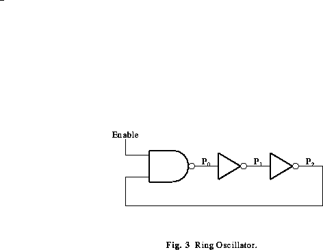
Because of the propagation delay through the gate, the state of
![]() at time t is actually a function of the state of the gate
inputs at time
at time t is actually a function of the state of the gate
inputs at time ![]() , where
, where ![]() is the propagation delay
through
the gate.
That is:
is the propagation delay
through
the gate.
That is:
![]() =
= ![]()
Hence, after one gate delay from the moment Enable becomes equal to 1,
![]() becomes equal to 0. One gate delay later,
becomes equal to 0. One gate delay later, ![]() changes
to 1, and so on. Let
changes
to 1, and so on. Let ![]() be the instant at which Enable changes
from 0 to 1. The sequence of events may be described as follows:
be the instant at which Enable changes
from 0 to 1. The sequence of events may be described as follows:
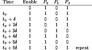
This sequence of events will repeat indefinitely, producing
oscillatory signals at ![]() , and
, and ![]() .
.
The ring oscillator circuit may be used to obtain the gate propagation
delay, ![]() , by measuring the oscillator's frequency. Design and build
a circuit to do so as follows:
, by measuring the oscillator's frequency. Design and build
a circuit to do so as follows:
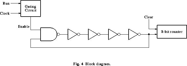
The required measurements are easily done with the equipment available in the laboratory if you choose n = 13 and a time period equal to one cycle of the built-in oscillator of your setup. Use two 4-bit counter chips (74LS193) to build an 8-bit counter to count the number of pulses. A block diagram for the required circuit is shown in Figure 4 for n = 5.
If you have LogicWorks, you should try to first simulate your circuit. The 74193 is available in the 7400 library. It will help you make sure that you have made the correct connections to the chips. You will have to add some delay to the gates in the ring.
The built-in oscillator has a period of about 20-25 ![]() when a 10pF timing
capacitor is used, but the frequency of oscillation may vary substantially.
You must take into account
about 20pF of parasitic capacitance for the timing capacitor
when using the timing period formula given in the sheet.
The parasitic capacitance is due to effects such as the protoboard
connections and the wires.
This will vary from board to board.
Under what conditions will the formula be usable without worrying
about the parasitics?
when a 10pF timing
capacitor is used, but the frequency of oscillation may vary substantially.
You must take into account
about 20pF of parasitic capacitance for the timing capacitor
when using the timing period formula given in the sheet.
The parasitic capacitance is due to effects such as the protoboard
connections and the wires.
This will vary from board to board.
Under what conditions will the formula be usable without worrying
about the parasitics?
If a logic analyzer is available, you can use it to obtain a more accurate value of the length of the clock cycle. What other ways are there to obtain the clock cycle?
Do your measurement several times and average the results. Why is this a good practice?
Change your circuit by adding a few more inverters, and redo the measurements.
The data sheet for a 74LS04 is included. The delay for a 74LS00 is similar. How do your results compare? If your results disagree, where might the problems lie?