PLEASE CHECK
OUR OPENINGS LISTINGS FOR MORE UP-TO-DATE INFORMATION
Research
goal
The main goal of our research program is to help
maintain and improve health by providing medical doctors, biomedical
researchers and/or patients with novel microelectronic
technologies for miniature medical devices that directly or indirectly
interface with the human body in order to monitor its function and, in some
cases, influence it. We also target scientific, industrial, consumer and
environmental sensory electronics applications.
Motivation
Modern healthcare practices suggest that
patient-interfacing medical devices of the future are to be potent, ubiquitous,
and inexpensive. Our research investigates such medical devices. These devices
address specific unmet healthcare needs, particularly those in medical monitoring, diagnostics and therapy
in clinics, biomedical research labs and at home. Of our immediate interest are
applications in neuroscience and molecular biology.
We target disorders and diseases with limited conventional treatment options or
with costly diagnostics options. Specific medical applications include
electronic therapy for intractable epilepsy [J21, C51, C56, J13] and electronic screening
for early detection of certain types of cancer [C45, C50, J16, J27, J28, J11, J15, J24].
Approach
Interfacing with the human body for the purpose of
maintaining or improving health requires a variety of sensory functionalities.
These can be as simple as monitoring key vital signs, or as complex as
monitoring electrochemical activity of the brain or examining biochemical
content of bodily fluids. In our research we target applications
where novel implantable, wearable or disposable biomedical devices with complex
sensory functions are uniquely enabled by low-cost integrated circuit (IC)
technologies such as CMOS.
Specifically, we focus on the design of integrated
circuits, VLSI architectures and signal-processing algorithms that comprise the
core of a sensory medical device. Such
sensory devices not only acquire raw sensory data, but also perform local
sensory signal processing (such as feature extraction and machine learning data
classification algorithms), and provide feedback information or, in some cases,
feedback action as shown in Figure 1. One successful example of such a system
is a single-chip brain implant for treatment of intractable epilepsy we
developed that accurately detects early seizures and automatically triggers
neuro-stimulation to effectively control them [J21, C51, C56].
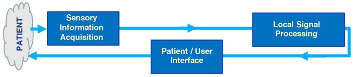
Figure 1. Functional block diagram of a biomedical
sensory microsystem.
Key
challenges
From the system integration
perspective, for potency, ubiquity and low cost it is often advantageous
to utilize sensory properties of the integrated circuits themselves or
additional small sensors of a similar form-factor, without bulky externally
connected sensors or associated packaging costs. In our previous work, we have
demonstrated suitability of silicon integrated
circuits (ICs) to be further integrated
(post-CMOS) with various arrays of on-die sensors for implantable,
wearable and disposable microsystem implementations. These include: implantable
arrays of micro-needles to monitor spatial maps of electrical neural activity
in the brain for epileptic seizure propagation studies [J9,
C27, J26, J7,
J12, J25] (e.g., in Figure 2, left);
arrays of gold microelectrodes to electrochemically measure concentration of
neurochemicals for brain chemistry studies [J35, J17, C37,
J5] or DNA concentration for cancer
screening [C45, C50, J16, J27, J28] (e.g., in Figure 2,
middle); and photo-detector arrays for optical contact-imaging of various
micro-scale biological objects such as fluorescently labeled DNA
microarrays [J11, J15, J18, J23, J24] (e.g., in Figure 2, right).
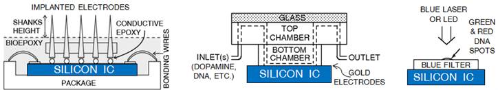
Figure 2. Examples of system integration solutions
with on-silicon sensors.
From the front-end circuits
perspective, the key challenges are low signal-to-noise ratio,
signal offset and drift, high interference levels, intrinsic electronic noise,
time-varying signal source properties, various artifacts and numerous other
sensory interface-related issues. In our previous work, we have addressed these
issues individually by sensory transducer
innovations (e.g., novel photodetectors [J15, J23]) and various integrated circuit design solutions (e.g.,
novel signal filtering circuits [J6, J20] and novel chopping circuits [J19, J23]). Our latest projects
include optical sensors for computational photography, electro-physiological
sensors for brain activity monitoring and modulation as well as
electro-chemical sensors for molecular diagnostics and neurochemistry
monitoring.
From the back-end circuits
perspective, the key challenges are the ever-growing requirements
for higher sensory signal processing throughput and higher integration density
with a limited power budget. Power budget is often
constrained by heat dissipation (such as that into the surrounding tissue). In
our previous work, we have developed a number of circuit
design techniques that break the conflicting throughput-area-power trade-offs.
These include various analog-to-digital converter architectures that perform
computationally-expensive signal processing operation such as multiplication
without a significant resource overhead and requiring no power- or area-hungry
digital multipliers [J6, J10,
J16, J20], as well as novel
energy-efficient signal processing mixed-signal VLSI architectures [J8, J13, J14, J20], low-power RF transceivers [J20, J21, J27, C45, C50], and wireless energy transfer [C55]. Within this thrust, we are currently
pursuing research in energy-efficient digital and mixed-signal accelerators for
high-performance machine learning and artificial intelligence applications,
computing architectures co-integrated with sensory arrays, as well as data and
energy transfer with on-CMOS inductive coils.
