256Kb DRAM Design
We designed a 256Kb DRAM using 0.35 technology. Using 8 multiplexed inputs to cover 32k of addresses (256 rows and 128 columns), each address corresponds to an 8-bit data. The memory core consists of 8 banks each providing one bit of the 8-bit data.
Our design is basically made from the following blocks : Control Logic Unit, Refresh Circuitry, Latches, Row Decoder, Column Decoder, Memory banks and Sense Amplifiers.
Row Decoder : An 8 to 256 decoder which drives the memory banks through the wordline buffer. We used pre-decoding to minimize the height of the row decoder to match twice of the height of memory cell. The row decoder is implemented by cascading 4 to16 decoders. The delay of the decoder is below 2ns when driving the big capacitive load of the memory wordlines.
Column Decoder : A 7 to 128 decoder which connects the desired bitlines (one from each memory bank) to the data buffers. We used pre-decoding to minimize the height of the column decoder to match twice of the width of the memory cell. The column decoder is implemented by cascading a 3 to 8 decoder and 4 to 16 decoders.
Latches : Provide the addresses and their complements for the decoders using the Control Logic Unit signals and the input multiplexed addresses.
Memory Banks : We have 8 memory banks each corresponding to 1 bit of data. To achieve minimum area, we have 256 polysilicon wordlines and 128 metal bitlines. Each memory cell has a 2.9 × 3.05 = 8.84 μ2 area. The storage capacitor is a MOS Cap with a capacitance of 1.4 fF. An array of Sense amplifiers comes on the top and bottom of each bank. The row and column decoders managed to be fitted just on one side of the memory.
Control Logic Unit : Using input control signals (like RAS, CAS and refreshing inputs), this unit produces the internal control signals. As an example, the logic unit activates the sense-amplifiers at the appropriate time or enables the decoders and I/O buffers at specific times required.
Sense Amplifier: This block is responsible for sensing the small voltage difference between two selected bitlines and amplifying this difference to produce “one” in one bitline and “zero” in another. During this procedure the cell previous voltage is also written back to (in read cycle). Layout of the sense amplifier should be as symmetric as possible. Since the cell width was quite small we decided to have two rows of sense amplifiers for each bank with twice of the pitch of the cell.
Refresh circuitry: DRAM should be refreshed periodically, since the storage capacitances will discharge because of leakage currents. We simulated the circuit and found out that we need refreshing every 2ms. The refresh circuitry consists of a counter which produces the row addresses and the rest of the circuit is the same. At refresh time, the output address of the counter is fed into the decoders and the clock is used as the new CAS. In every cycle, a row is selected and all the cells connected to that row are read and written back to. Totally the memory is available for more than %99.85 in time.
Padframe : The number of pins is 29 including 4 vdd pins and 4 gnd pins. There are 5 pins for RAS, CAS, RD/WR and two for the refresh circuitry. There are also 16 pins for data and addresses, 8 pins each.We used some input PADS and designed the I/O pads for input/output data.
The chip area including the padframe is almost 1.8 mm2 .
Timing specifications: Set up time(the interval that the address should be valid before RAS or CAS coming down) is equal to zero since the address is taken some time after falling edge of RAS or CAS. Hold time is equal to 1.7 ns. Minimum CAS interval is 6.5 ns and reading data is valid to 3ns after CAS goes high. After CAS goes high, RAS should remain low at least 3.1ns. After this interval RAS should go high and remain high for at least 3ns so that the circuit gains its equilibrium conditions (bitline voltages reach the same value).The data is valid 8.8 ns after CAS goes low. The following figure shows the timing of a read cycle. Writing cycle is the same except that the desired data should be valid at the interval marked ”valid data” to be written into the cell properly.
Total chip area including the padframe is almost 3.24 mm2 (1.8mm by 1.8 mm) and the maximum speed is 60 MHz.
Following figures show the timing diagram and the schematic and layout of the whole chip.
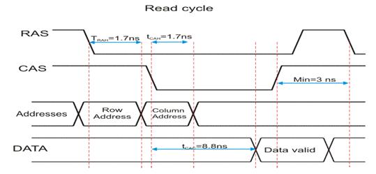
Figure 1. Timing diagram of a read cycle
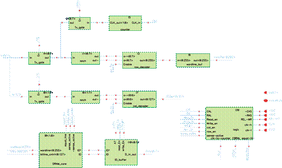
Figure 2. Schematic view of the DRAM circuit blocks.
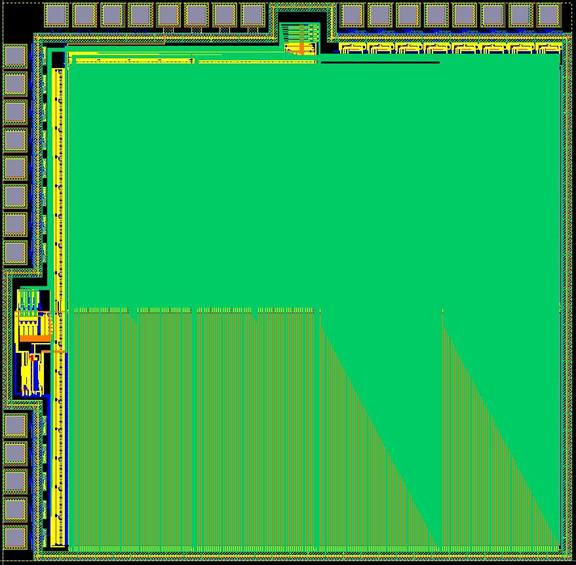
Figure 3. DRAM chip layout.