A direct digital synthesizer (DDS) generates waveforms by reading an internal/external lookup table or by calculation with appropriate algorithms. Generation of sine waves is usually the main use of a DDS. Output waveforms and frequency are inherently accurate as long as the clock frequency supplied to the DDS and the waveform stored in the lookup table or the waveform calculation algorithm are accurate. For IF demodulation, quadrature waves (sine and cosine waves of the same frequency) are often used for image rejection purposes, and accurate phase between sine and cosine waves is very important for good image rejection. The phase accuracy is also easily obtained with a DDS. However, the output of a DDS has to be carefully filtered in order to remove quantization noises.
This project involves design of a direct digital synthesizer with an internal lookup table of a sine wave with digital
sine and cosine outputs. The original plan was to include an A/D converter and digital multipliers for demodulation.
However, they were removed due to designer's insufficient ability and the limited
time.
Specification of the DDS
| Clock Frequency | 8.192 MHz |
| Frequency Step | 1 kHz |
| Target Output frequency range | 1 kHz-2MHz |
| Frequency control word length | 12 bits |
| Output word length | 8 bits |
The target output frequency is from several hundred KHz to 2 MHz. This range includes 455KHz, which is often used
for IF of radio voice, and carrier frequency of the AM radio. Therefore, this DDS may be used for IF demodulation or direct
demodulation of the AM radio signals. The clock frequency is equal to the sampling frequency of the sine waveform in the lookup table. For frequency control
purposes, it is desired that the sampling frequency (=clock frequency) be frequency step
X 2^n. 4.096 MHz sampling rate is the minimum required sampling rate for 2MHz output.
Therefore, 8.192 MHz was chosen to relax the filter specification.
8-bit output word length is sufficient for voice demodulation purposes.
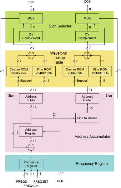
The following shows the block diagram of the system. The address accumulator counts the address of the
ROM (sine wave lookup table) by adding the content of the frequency register. Address of the ROM corresponds to the phase of the sine
wave. If, for example, the frequency register contains 1, the address increases by 1 at each clock making 1 kHz output.
However, if the input is 2, the address is increased by 2. This results in the doubled frequency, which is 2 kHz. The two
ROMs are identical but addressed differently for 90-degree phase shift. The ROM contains a 1/4 stroke of a sine wave
instead of a full stroke to save area. Therefore, the address accumulator requires extra logics that "fold" the address and take 2's
comlement when necessary.
System Diagram
The sine lookup table contains a 1/4 stroke of a 1kHz sine wave instead of a full stroke for area reduction. The remaining 3/4 stroke can be generated by copying the first 1/4 stroke. Therefore, the lookup table needs 2048 7-bit words instead of 8. For further are saving, a very simple compression algorithm known as Hutchison Algorithm was used. This algorithm makes use of the fact that the sine wave is smooth and monotonically increasing/decreasing for each 1/4 stroke. The waveform is constructed with two lookup tables: a coarse ROM and a fine ROM. The coarse ROM contains the waveform at lower sampling rate with the original resolution.
The fine ROM contains the waveform at the original sampling rate with low resolution. Adding the fine data and coarse data together results in the original waveform without any loss of information. The drawback of this algorithm is that an additional adder and decoders are required. Compression rate depends on the sampling rate ratio (coarse sampling rate/original sampling rate) of the coarse ROM and resolution of the fine ROM. The down sampling rate should be 1/2^n to ease coarse addressing. For this project, 1/8 sampling frequency for the coarse ROM and 1-bit resolution for the fine ROM were found to be optimal. Without compression, the DDS of this project requires 28,672 bits. However, with the compression algorithm, the size is reduced to 7,680 bits. Diagrams of the fine and coarse ROMs are shown below.
Diagrams of the fine ROM and the Coarse ROM
The address accumulator counts address(phase) of the lookup table according to the frequency specified by the frequency register. The accumulator simply adds the content of the frequency register to the value of the current address register. The address register contains 13-bit address(0-8,191) which is for full-stroke adressing. The following address folder convert this 13-bit address to 11-bit address for 1/4 stroke addressing. The address folder outputs sign flag which is connected to the multiplexer that selects sign of the output. Converting address of sine to cosine is easy; add 2,048 to the address.
The frequency register simply stores frequency in kHz. It accepts inputs from a simple serial interface.
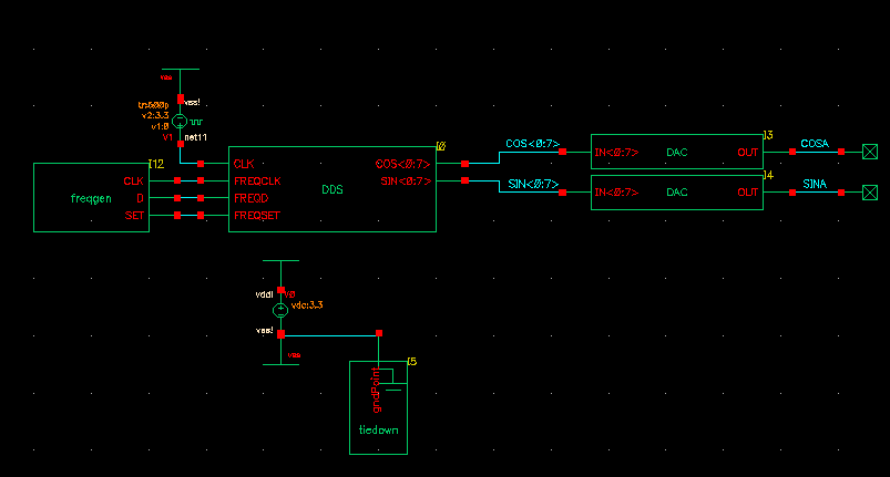
TSMC CMOS 0.35um technology was used for design of this project. Schematic design and simulation were done with Virtuoso Schematic Composer and Analog Artist Mixed-Signal Environment, respectively. All of the blocks except for the ROMs were designed in static logic. The following figure shows the top level schematic (excluding the padframe) of the DDS.
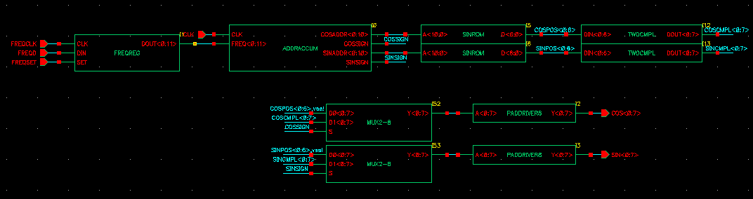
Top Level Schematic of the DDS
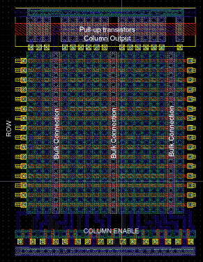
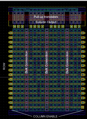
The sine lookup table consists of two identical ROMs, and each ROM contains a coarse ROM and fine ROM. The NAND-ROM structure was adopted rather than NOR-ROM in order to save space. Both the coarse ROM and the fine ROM consist of columns of series transistors. Each column represents 16-bit data, and it consists of series connected transistors (representing '0') and metal wire (representing '1'). One end of the column is a column enable transistor which is tied to the ground and the other is connected to a weak pull-up transistor. The following figure shows one column of NAND-ROM with 8 rows instead of 16 for simplicity.
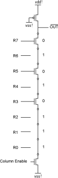
The top PMOS transistor is the weak pull-up. This transistor has to weak because many transistors are connected in series. when column enable is low, the output is always high. All unselected rows are high, and only the selected row is pulled low. If the selected row is a transistor, the path to vss is cut with the transistor and the output is high. However, if it is a metal wire, the output is low because all other rows are conductive.
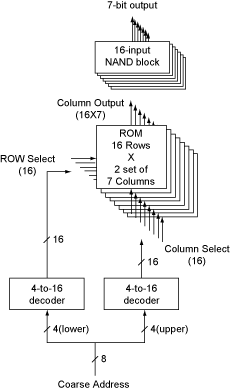
The coarse ROM contains 1792 bits of data. There are 16 sets of 7-bit-wide columns, and each column consists of 16 bits (rows). Therefore, a 4-to-16 decoder that selects one set out of 16 sets of 7 columns and another 4-to-16 decoder that select a row out of 16 rows are required. The row decoder has to be strong enough to drive many transistors (up to 112 transistors). Therefore, a predecoded decoder was chosen to save space. Both the decoder should be in similar width for better layout.
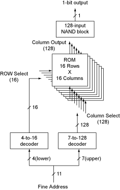
The Fine ROM contains 2048 bits of data. There are 128 columns containing 16
bits (rows). Therefore, a 7-to-128 decoder,
4-to-16 decoder, and a 128-input NAND block are required. To save space, the 7-to-128 decoder was chosen to be a predecoded one.
The same 4-to-16 decoder of the Coarse ROM was used for the fine ROM.
The address accumulator consists of an adder, address
register (D-FFs), and a address folder. The adder is a normal ripple carry
adder the delay of this adder actually does not affect the performance of the system as long as it can perform addition
within one clock cycle which is about 122 ns. At each clock, data from the frequency register is added to the value of the address register and the result is stored
in the address register. The D-FFs are normal ones with four pass-transistors. The address folder folds 13-bit address
into 11-bit address as 0-8191 -> 0-2047-0-2047 and generates the sign signal. This was first described in behavioral Verilog codes,
and it was found out that this behavior can be simply implemented with a few XOR gates. Sine cosine address conversion is done
with one two-input XOR and an inverter. The following figure shows
the schematic.
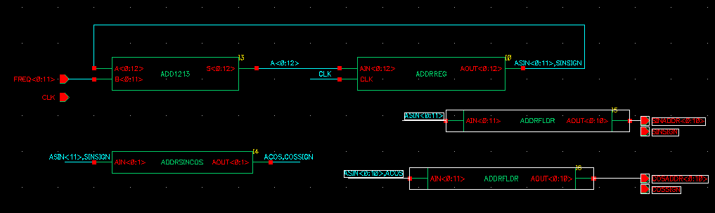
Schematic of Address Accumulator
Frequency Register consists of consists of two 14-bit registers. The first one is a shift register that accepts a serial input for
frequency change, and the second one is the actual register that is read by the address accumulator. The SET signal writes the data
in the first stage to the second stage so that the output frequency does not change until the new frequency is completely loaded.
The sign selector selects either negative or positive data according to the sign input with multiplexers.
The negative data is generated by inverters and half adders to take 2's complement.
Since the buffer inside the output pads is large, a smaller buffer was added.
All blocks were first tested in transistor level with a dummy load. After checking functions, they were switched to Verilog behavioral models in order to reduce simulation time. However, most of the blocks are described with combination of many low-level behavioral models such as those of inverters, NANDs, D-FFs, and so on in order to avoid design mistakes. SpectreSVerilog simulator allows users to place instances described in Verilog or Verilog-A with other transistor-level blocks for mixed-signal simulation. For example, it took five hours to run one simulation to check the ROM in transistor-level. The same simulation with Verilog models takes less than a minute. For the final simulation, in order to see the actual wave forms, a DAC instance described in Verilog-A was connected to the DDS consisting of many Verilog instances. The Verilog-A code were automatically generated by Cadence ModelWriter. The following figure shows the result of one simulation. The frequency was changed from 455kHz to 1MHz at t=7.5us. This simulation took less than one minute despite the complexity of the circuit (over 10,000 transistors) thanks to the mixed-signal environment.
Testbench
.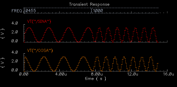
Simulation Results
All the layout was done manually. Unfortunately most of the time was spent for the ROM due to its non-uniform structure. Dimension of the entire design including the pad frame is 972um X 670um. Layouts of some important blocks are shown below.
 |
 |
| Part of Fine ROM | Part of Coarse Rom |
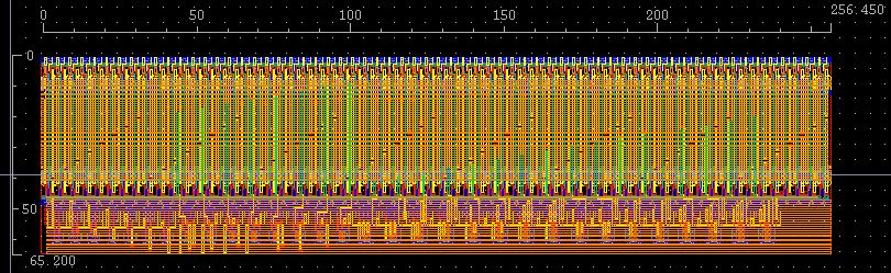
7-to-128 Decoder with a predecoder
The bottom part is the predecoder. The predecoded lines run horizontally over the yellow region. There are 64 NOR gates on top and another 64 NOR gates at the bottom of the yellow area.
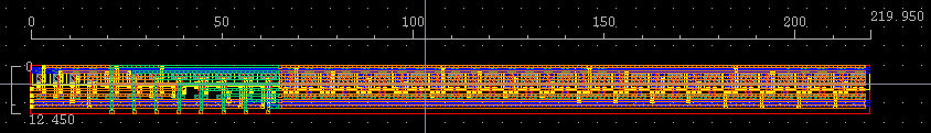
4-to-16 Decoder with a predecoder
The left half is the predecoder, and the right half contains 16 NOR gates.
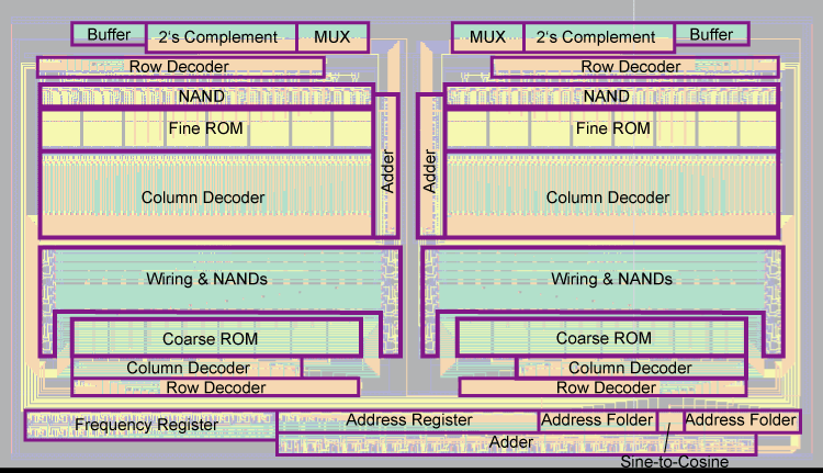
Floor Assignment of the Core
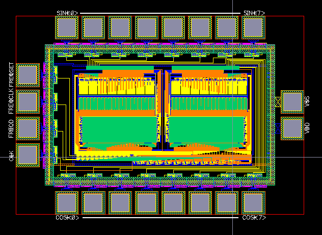
The Entire Layout
[EOF]