CMOS Image Sensor with
High-Speed Column-Parallel Two-Step Single-Slope Analog-to-Digital Converter (ADC)
and JPEG Compressor
ECE 1388 Final Report - Winter 2016
Zhang Yuqing - M. Eng. Energy Systems
Liu Yanhui - M. Eng. Energy Systems
Zhao Minghua - M. Eng. Electronics
Li Ziming - M. Eng. Electronics
Fan Yinze - M. Eng. Energy Systems
2.1.2 Correlated Double Sampling (CDS)
2.1.3 Analog to Digital Converter (ADC)
Elaboration on
Essential Components
3.1 Group Final Project
Attribution Table
3.4 Analog to Digital Component
Connectivity
3.8 Geometry
Verification for Digital Components
3.8.1 Control Module
(Generated by Encounter)
3.8.2 Counter 8 (Generated
by Encounter)
3.8.3 Counter 9
(Generated by Encounter)
3.8.4 Decoder 8’bit
to 256 bit (Generated by Encounter)
3.8.5 JPEG encoder
(Generated by Encounter)
3.8.6 Column
Multiplexer (Generated by Encounter)
3.8.7 Subtractor 8 bits
(Generated by Encounter)
3.9 Complete analog LVS report
1. Functional Specification
This report examines the design process, implementation, and testing of a Two-Step Single-Slope Analog to Digital Converter using IBM 0.13µm technology. The analog section includes a pixel array, a correlated-double sampling component, and a column parallel two-step single slope ADC. The ADC is used to process analog inputs in the range of 0.5V to 1.5V. More details could be found in the datasheet Table 2 in the Appendix. The pixel bitstream is assembled with a row decoder and a column multiplexer. The JPEG compressor module takes 8’bit pixel as input and outputs 32-bit bitstream of JPEG data.
2. Chip Design
This section describes the chip in terms of the modular structure shown in the top-level architecture diagram Figure 1 in the Appendix. The entire chip layout Figure 2 is available in the Appendix.
2.1 Analog Subsection
2.1.1 Pixel
Array
Each pixel has 4 transistors. A 4T pixel is a variation of the standard 3T pixel, aimed at solving various noise issues (mainly KTC noise) with 3T pixels. Because the pixel array conforms to the QVGA resolution, the size of pixel array is 320x240. The detection node gets separated by using an additional transistor between the photodiode and the source follower. A shared pixel design is also used in pixel array. The shared architecture has only one readout circuit and the structure of 4T shared pixel is shown in Figure 5.
2.1.2 Correlated
Double Sampling (CDS)
Due to the differences in adjacently located circuit components, photodiodes are no longer identical and the fixed pattern noise will be induced. Fixed Pattern Noise (FPN) is a major factor causing the degradation of image quality in CMOS image sensor. To suppress the noise and improve the image quality, a correlated double sampling circuit is introduced. Structure of CDS circuit is shown in Figure 6. The CDS circuit consists of one op-amp, two analog switches and two capacitors. To cancel out the noise, the CDS circuit samples two voltages (reset voltage and signal voltage) which includes noises successively and subtract each other to get the desired signal value.
2.1.3 Analog
to Digital Converter (ADC)
Single slope ADC provides better trade off among complexity, power consumption, and area. However, each n-bit takes 2^n clock periods for conversion. In order to increase this speed, Two-Step Single Slope ADC has been implemented in the design which improves the conversion time to 2^(n/2)+2^(n/2). The conversion process can be divided in two steps: coarse and fine phases. ADC architecture is shown in Figure 7. Each column circuitry includes a comparator, two memory blocks, a multiplexer and a decoder. The simplicity of the column circuitry can minimize column fixed-pattern noise (FPN). The ADC operation overview is described below.
Top Level Operation
In the coarse phase, the MUX changes to high - output is selected so it connects the coarse counter to the decoder. The ramp and reference generator generates a constant voltage (reference voltage 1.5V), and 16 reference signals counting down from 1.5V to 0.5V (ramping voltage). Both the constant voltage and the reference signals are input to the comparator. When the difference of ramping voltage and reference voltage exceeds the pixel signal voltage from the CDS, the comparator changes outputs state high. This causes the counter value to be stored in memory and fed back into the reference generator for the next phase.
In the fine phase, Mux changes to low, 4-bit coarse memory data obtained from last phase is connected to decoder to select the corresponding reference voltage to comparator. The ramping generator generates a ramping signal from 1.4375V to 1.5V,which is synchronous with counter. Comparator changes state to high when differential voltage between ramping and reference exceeds the signal voltage.
Finally a subtractor is used to merge two 4-bit data to one 8-bit data by subtracting the coarse and fine 4-bit values. The coarse value takes the most significant 4 bits followed by four zero bits. The fine value occupies the least significant four bits with four zeros as most significant bits. The resulting 8 bit data is fed to the JPEG compressor.
Elaboration
on Essential Components
The reference generator is implemented based on a resistor string. A string of sixteen equal resistors, connected between two reference voltages (1.5V and 0.5V) , acts as voltage dividers to generate sixteen reference voltages. Then the reference voltages are buffered by a two-step differential amplifier to drive all the column circuits. Again, the comparator changes to high when differential signal exceeds signal voltage.
The comparator in this project consists of a three-stage preamplifier and a latch. The Preamplifier uses folded fully differential amplifiers. Dynamic offset cancellation technique is applied by association with 4 pairs of capacitors. With the proper control of switches, the comparator takes the difference between the ramping signal and reference voltage, and compares that with the signal voltage. The timing diagram of four switches are shown in Figure 42. The waveform of ramping and reference generators are shown in Figure 49. The comparator specification is shown in Figure 8.
2.2 Digital Subsection
The digital subsection is composed of the following components: Control Logic, and JPEG compressor. The Control Logic selects the pixels from the pixel array row-by-row. The row of pixels are in turn fed into the CDS, ADC, and Multiplexer sequentially in parallel. The Multiplexer will then feed each 8’bit pixel of the row one by one to the JPEG compressor module. The JPEG compressor was designed by David Lundgren and the verilog code was taken from OpenCores. It module takes in 8x8 blocks of pixels at a time, waits 33 clk, resets the enable signal for one clock cycle, and repeats until the end of array. It outputs a 32’bit bitstream of ready-to-save bits. For proper operation of the JPEG compressor, the pixel array data should be stored 8x320 pixel buffer so that 8x8 blocks can be entered one at a time as the next 8x320 digital pixel data are generated. Due to the scope and time constraints of the project, the buffer was not implemented. The JPEG compressor finishes, an end-of-file signal will rise.
2.3 Pad Frame
The pad frame is divided into digital and analog sections with individual ground buses. Figure 2 shows the layout of complete chip. There are 35 pins including 32 bit stream from JPEG compressor, analog ground, digital ground and vdd.
3. Appendix
List of Tables:
Table 1: Group Final Project Attribution Table
Table 2: Specifications of Chip
Table 3: Specifications of ADC
Table 4: Analog to Digital Component Connectivity
List of Figures:
Figure 1: Top-level Architecture Diagram
Figure 2: Complete Chip Layout
Figure 3: DRC report of Analog portion
Figure 4: LVS report of Analog portion
Figure 5: 4T - Shared Pixel
Figure 6: Correlated Double Sampling
Figure 7: ADC column circuitry
Figure 8: Comparator
Figure 9: Pre Amplifier (Folded Fully Differential Amplifier)
Figure 10: Latch
Figure 11: Memory top-level
Figure 12: 1 Bit Memory Cell
Figure 13: Multiplexer
Figure 14: 16 Bit Decoder
Figure 15: 4-Bit Counter
Figure 16: Ramping and Reference Generator
Figure 17: JPEG compressor top-level module (by Design Vision)
Figure 18: 8-bit Row Decoder (by Design Vision)
Figure 19: 9-bit Row Decoder Column Counter (by Design Vision)
Figure 20: Mux
Figure 21: Control Logic Module
Figure 22: 8'b counter
Figure 23: 9'b counter
Figure 24: Pixel Array
Figure 25: Correlated Double Sampling
Figure 26: Complete analog ADC (Column Circuitry and reference &
ramping generator)
Figure 27: Comparator
Figure 28: Pre Amplifier (Folded Fully Differential Amplifier)
Figure 29: Latch
Figure 30: Memory
Figure 31: Multiplexer
Figure 32: 4 to 16 Bit Decoder
Figure 33: 4-bit Counter
Figure 34: Ramping and Reference Generator
Figure 35: JPEG compressor - full layout
Figure 36: 8-bit Row Decoder
Figure 37: Mux
Figure 38: 8'b counter
Figure 39: control logic
Figure 40: 9'b counter
Figure 41: Correlated Double Sampling
Figure 42: Comparator (a)
Figure 43: Comparator (b)
Figure 44: Memory
Figure 45: Multiplexer
Figure 46: 4 to 16 Bit Decoder
Figure 47: 4-bit Counter (Count-down)
Figure 48: 4-bit Counter (Count-up)
Figure 49: Ramping Generator
Figure 50: Reference Generator
3.1 Group Final Project
Attribution Table
Table 1: Group Final Project Attribution Table
|
Task |
Zhang Yuqing |
Liu Yanhui |
Zhao Minghua |
Li Ziming |
Fan Yinze |
|
Research |
|||||
|
ADC architecture and implementation |
X |
X |
|
|
|
|
Design, Schematic and Unit Testing |
|||||
|
Pixel array |
|
X |
|
|
|
|
Correlated double sampling |
|
X |
|
|
|
|
Ramp and reference generator |
|
|
|
|
X |
|
Comparator |
X |
|
|
|
|
|
4-bit memory |
|
|
|
X |
|
|
4-bit decoder |
|
|
|
X |
|
|
4-bit counter |
|
|
|
X |
X |
|
2 to 1 multiplexer |
|
|
|
X |
|
|
Control Logic (generated by Design Vision ) |
X |
|
X |
|
|
|
Column Multiplexer (generated by Design Vision) |
|
|
X |
|
|
|
Pixel array Row Decoder (generated by Design Vision) |
|
|
X |
|
|
|
JPEG compressor (from Opencores) |
|
|
X |
|
|
|
Layout and LVS |
|||||
|
Pixel array |
|
X |
|
|
|
|
Correlated double sampling |
|
X |
|
|
X |
|
Ramp and reference generator |
|
|
|
|
X |
|
Comparator |
|
|
|
X |
X |
|
4-bit memory |
|
|
|
X |
X |
|
4-bit decoder |
|
|
|
X |
|
|
4-bit counter |
|
|
|
X |
X |
|
2 to 1 multiplexer |
|
|
|
X |
|
|
Control Logic (generated by encounter) |
|
|
X |
|
|
|
Column Multiplexer(generated by encounter) |
|
|
X |
|
|
|
Pixel array Row Decoder(generated by encounter) |
|
|
X |
|
|
|
JPEG compressor (generated by encounter) |
|
|
X |
|
|
|
Circuit assembly |
|
|
|
X |
|
|
Core with pad frame |
X |
X |
|
|
|
3.2 Top-level Architecture
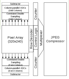
Figure 1: Top-level Architecture Diagram
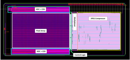
Figure 2: Complete Chip Layout
3.3 Final Chip Specification.
Table 2: Specifications of Chip
|
Pixel Array Resolution |
320 x 240 - QVGA |
|
Padframe Size |
8.50 mm x 3.86 mm |
|
Operating Clock Frequency (ADC) |
50 MHz |
|
Operating Clock Frequency |
100 MHz |
|
Power Consumption (ADC) |
60 mW |
Table 3: Specifications of ADC
|
Parameter |
Value |
|
Column pitch |
30 µm |
|
Process |
GF 0.13 µm |
|
Supply |
3.3V |
|
ADC resolution |
8 bit |
|
ADC conversion time |
0.64usec |
|
Pixel output signal range |
0.5V – 1.5 V |
|
frequency |
50 MHz |
3.4 Analog to Digital Component
Connectivity
Table 4: Analog to Digital Component Connectivity
|
Block - output (pin
name) |
Block - input (pin
name) |
Explanation |
|
counter8 - out[0:7] |
decoder8_256 - a[0:7] |
select pixel array row by row |
|
counter9 - out[0:8] |
mux2650 - select[0:8] |
select pixel of each row |
|
ADC - Course 4’b output |
sub8 - dataa[0:3] |
subtract course with fine (dataa - datab) |
|
ADC - Fine 4’b output |
sub8 - datab[0:3] |
|
|
sub8 - result [7:0] (x320) |
mux2560 - [0:2559] |
ADC result into Mux (or column decoder). These are not wired as there are too many wires to place manually, and the input pins of the multiplexer (2560 input pins in total) were ordered randomly by encounter when generating the layout. |
|
VDD/VSS - for all digital blocks |
|
Digital metal stripes on lower left corner: horizontal row 1 is VSS; horizontal row 2 is VDD |
|
mux2560 - q[0:7] |
JPEG compressor- data_in [0:23] ( q[0:7] -> data_in [0:7], q[0:7] -> data_in[8:15], q[0:7] -> data_in[16:23] ) |
Pixel connection |
|
control_logic - c8_e |
counter8 - enable |
Enable counter |
|
control_logic - c8_r |
counter8 - reset |
reset counter to 0 |
|
control_logic - c8_c |
counter8 - clock |
positive edge of this clock makes counter +1 |
|
control_logic - c9_e |
counter9 - enable |
enable counter |
|
control_logic - c9_r |
counter9 - reset |
reset counter to 0 |
|
control_logic - c9_c |
counter9 - clock |
positive edge of this clock makes counter +1 |
|
decoder8_256 - w[0:239] |
pixel array - row 1 to 240 |
|
|
jpeg_top - JPEG_datastream[31:0] |
Pad frame - output pins |
Also, due to the random distribution of the 32 pins and the distribution of them over a large area of the chip, they were not wired as it would require too much manual work. |
|
Pad frame- external pins |
control_logic - clk, enable, reset |
Controls the operation of the entire image capturing process of the pixel array |
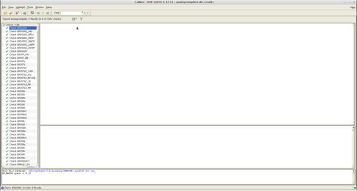
Figure 3: DRC report of Analog portion
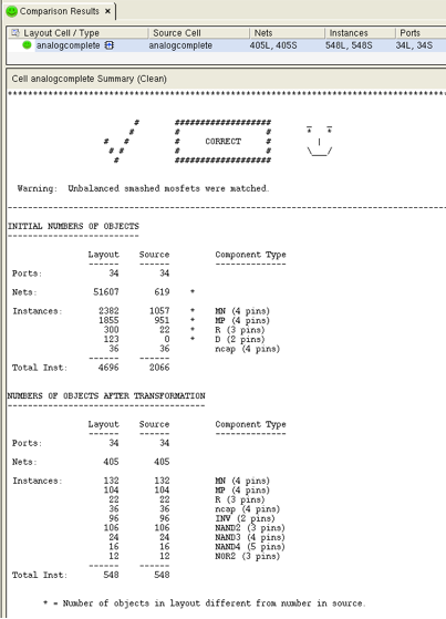
Figure 4: LVS report of Analog portion
3.5 Schematic
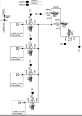
Figure 5: 4T - Shared Pixel
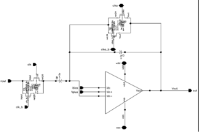
Figure 6: Correlated Double Sampling
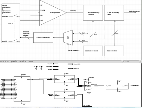
Figure 7: ADC column circuitry
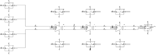
Figure 8: Comparator
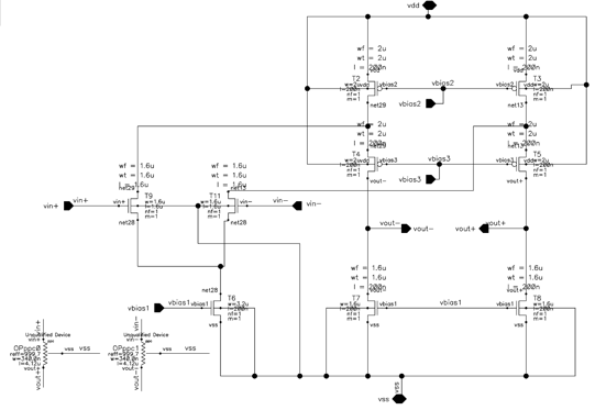
Figure 9: Pre Amplifier (Folded Fully Differential Amplifier)
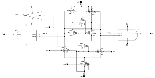
Figure 10: Latch
Figure 11: Memory top-level
Figure 12: 1 Bit Memory Cell
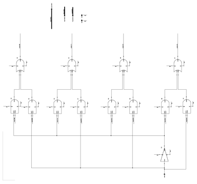
Figure 13: Multiplexer
Figure 14: 16 Bit Decoder
Figure 15: 4-Bit Counter
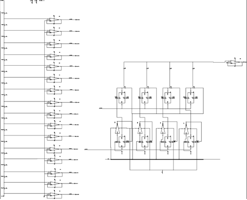
Figure 16: Ramping and Reference Generator
Figure 17: JPEG compressor top-level module (by Design Vision)
Figure 18: 8-bit Row Decoder (by Design Vision)
Figure 19: 9-bit Row Decoder Column Counter (by Design Vision)
Figure 20: Mux
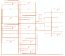
Figure 21: Control Logic Module
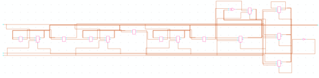
Figure 22: 8'b counter
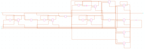
Figure 23: 9'b counter
3.6 Cell layout
Figure 24: Pixel Array
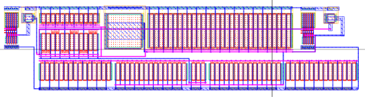
Figure 25: Correlated Double Sampling
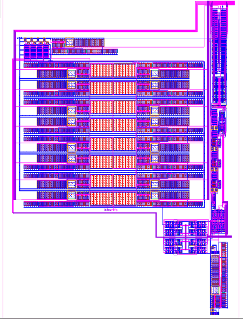
Figure 26: Complete analog ADC (Column Circuitry and reference & ramping generator)
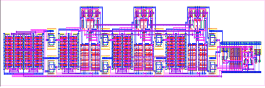
Figure 27: Comparator
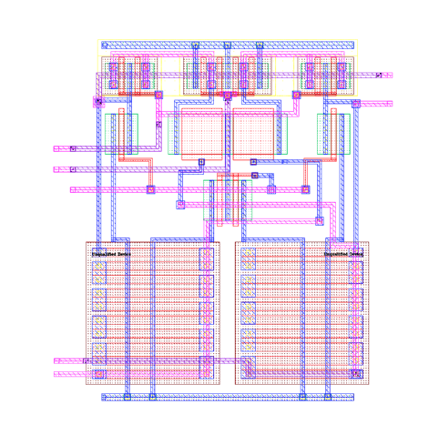
Figure 28: Pre Amplifier
(Folded Fully Differential Amplifier)
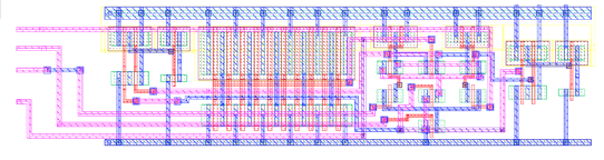
Figure 29: Latch
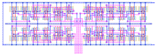
Figure 30: Memory
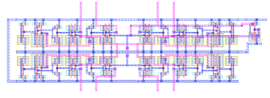
Figure 31: Multiplexer
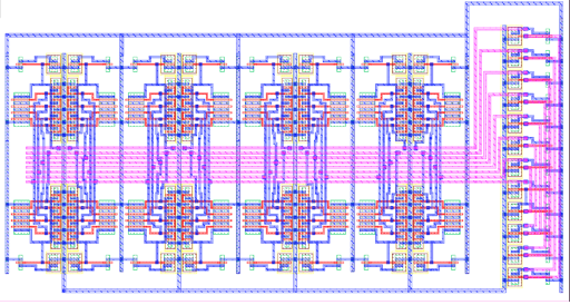
Figure 32: 4 to 16 Bit Decoder
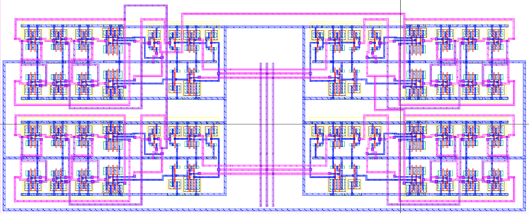
Figure 33: 4-bit Counter
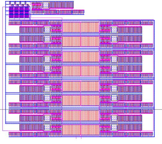
Figure 34: Ramping and Reference Generator
Figure 35: JPEG compressor - full layout
![]()
Figure 36: 8-bit Row Decoder
Figure 37: Mux
![]()
Figure 38: 8'b counter
![]()
Figure 39: control logic
![]()
Figure 40: 9'b counter
3.7 Simulation Waveform
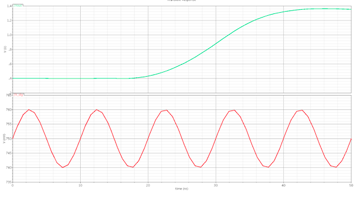
Figure 41: Correlated Double Sampling
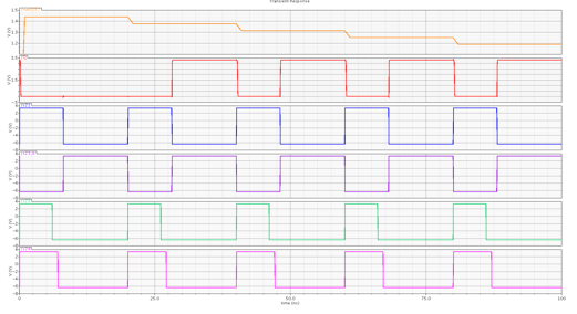
Figure 42: Comparator (a)
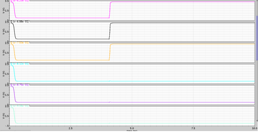
Figure 43: Comparator (b)
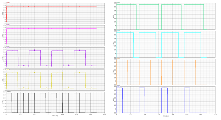
Figure 44: Memory
Figure 45: Multiplexer
Figure 46: 4 to 16 Bit Decoder
Figure 47: 4-bit Counter (Count-down)
Figure 48: 4-bit Counter (Count-up)
Figure 49: Ramping Generator
Figure 50: Reference Generator
3.8 Geometry Verification for Digital Components
3.8.1 Control Module (Generated by
Encounter)
Loading preference file control_logic.enc.dat/enc.pref.tcl ...
Loading mode file control_logic.enc.dat/control_logic.mode ...
loading place ...
loading route ...
<CMD> displaySpareCell
<CMD> setDrawView place
<CMD> verifyGeometry
*** Starting Verify Geometry (MEM: 567.9) ***
VERIFY GEOMETRY ...... Starting Verification
VERIFY GEOMETRY ...... Initializing
VERIFY GEOMETRY ...... Deleting Existing Violations
VERIFY GEOMETRY ...... Creating Sub-Areas
...... bin size: 2560
VERIFY GEOMETRY ...... SubArea : 1 of 1
VERIFY GEOMETRY ...... Cells : 0 Viols.
**WARN: (ENCVFG-47): Pin of Cell FILLER_impl0_49 at (2.000, 28.520), (3.000, 29.080) on Layer M1 is not connected to any net. Use globalNetConnect or GUI FloorPlan->Connect Global Nets to specify global net connection rules properly.
VERIFY GEOMETRY ...... SameNet : 0 Viols.
VERIFY GEOMETRY ...... Wiring : 0 Viols.
VERIFY GEOMETRY ...... Antenna : 0 Viols.
VERIFY GEOMETRY ...... Sub-Area : 1 complete 0 Viols. 0 Wrngs.
VG: elapsed time: 0.00
Begin Summary ...
Cells : 0
SameNet : 0
Wiring : 0
Antenna : 0
Short : 0
Overlap : 0
End Summary
Verification Complete : 0 Viols. 0 Wrngs.
**********End: VERIFY GEOMETRY**********
*** verify geometry (CPU: 0:00:00.1 MEM: 6.2M)
3.8.2 Counter 8 (Generated by Encounter)
Loading preference file counter8.enc.dat/enc.pref.tcl ...
Loading mode file counter8.enc.dat/counter8.mode ...
loading place ...
loading route ...
<CMD> displaySpareCell
<CMD> setDrawView place
<CMD> verifyGeometry
*** Starting Verify Geometry (MEM: 567.9) ***
VERIFY GEOMETRY ...... Starting Verification
VERIFY GEOMETRY ...... Initializing
VERIFY GEOMETRY ...... Deleting Existing Violations
VERIFY GEOMETRY ...... Creating Sub-Areas
...... bin size: 2560
VERIFY GEOMETRY ...... SubArea : 1 of 1
VERIFY GEOMETRY ...... Cells : 0 Viols.
**WARN: (ENCVFG-47): Pin of Cell FILLER_impl0_49 at (2.000, 28.520), (3.000, 29.080) on Layer M1 is not connected to any net. Use globalNetConnect or GUI FloorPlan->Connect Global Nets to specify global net connection rules properly.
VERIFY GEOMETRY ...... SameNet : 0 Viols.
VERIFY GEOMETRY ...... Wiring : 0 Viols.
VERIFY GEOMETRY ...... Antenna : 0 Viols.
VERIFY GEOMETRY ...... Sub-Area : 1 complete 0 Viols. 0 Wrngs.
VG: elapsed time: 1.00
Begin Summary ...
Cells : 0
SameNet : 0
Wiring : 0
Antenna : 0
Short : 0
Overlap : 0
End Summary
Verification Complete : 0 Viols. 0 Wrngs.
**********End: VERIFY GEOMETRY**********
*** verify geometry (CPU: 0:00:00.1 MEM: 6.1M)
3.8.3
Counter 9 (Generated by Encounter)
Loading preference file counter9.enc.dat/enc.pref.tcl ...
Loading mode file counter9.enc.dat/counter9.mode ...
loading place ...
loading route ...
<CMD> displaySpareCell
<CMD> setDrawView place
<CMD> verifyGeometry
*** Starting Verify Geometry (MEM: 567.9) ***
VERIFY GEOMETRY ...... Starting Verification
VERIFY GEOMETRY ...... Initializing
VERIFY GEOMETRY ...... Deleting Existing Violations
VERIFY GEOMETRY ...... Creating Sub-Areas
...... bin size: 2560
VERIFY GEOMETRY ...... SubArea : 1 of 1
VERIFY GEOMETRY ...... Cells : 0 Viols.
**WARN: (ENCVFG-47): Pin of Cell FILLER_impl0_49 at (2.000, 28.520), (3.000, 29.080) on Layer M1 is not connected to any net. Use globalNetConnect or GUI FloorPlan->Connect Global Nets to specify global net connection rules properly.
VERIFY GEOMETRY ...... SameNet : 0 Viols.
VERIFY GEOMETRY ...... Wiring : 0 Viols.
VERIFY GEOMETRY ...... Antenna : 0 Viols.
VERIFY GEOMETRY ...... Sub-Area : 1 complete 0 Viols. 0 Wrngs.
VG: elapsed time: 0.00
Begin Summary ...
Cells : 0
SameNet : 0
Wiring : 0
Antenna : 0
Short : 0
Overlap : 0
End Summary
Verification Complete : 0 Viols. 0 Wrngs.
**********End: VERIFY GEOMETRY**********
*** verify geometry (CPU: 0:00:00.1 MEM: 6.2M)
3.8.4
Decoder 8’bit to 256 bit (Generated by Encounter)
Loading preference file decoder8_256.enc.dat/enc.pref.tcl ...
Loading mode file decoder8_256.enc.dat/decoder8_256.mode ...
loading place ...
loading route ...
<CMD> displaySpareCell
<CMD> setDrawView place
<CMD> verifyGeometry
*** Starting Verify Geometry (MEM: 570.2) ***
VERIFY GEOMETRY ...... Starting Verification
VERIFY GEOMETRY ...... Initializing
VERIFY GEOMETRY ...... Deleting Existing Violations
VERIFY GEOMETRY ...... Creating Sub-Areas
...... bin size: 2560
VERIFY GEOMETRY ...... SubArea : 1 of 1
VERIFY GEOMETRY ...... Cells : 0 Viols.
**WARN: (ENCVFG-47): Pin of Cell FILLER_impl0_2605 at (0.000, 1500.920), (1.000, 1501.000) on Layer M1 is not connected to any net. Use globalNetConnect or GUI FloorPlan->Connect Global Nets to specify global net connection rules properly.
VERIFY GEOMETRY ...... SameNet : 0 Viols.
VERIFY GEOMETRY ...... Wiring : 0 Viols.
VERIFY GEOMETRY ...... Antenna : 0 Viols.
VERIFY GEOMETRY ...... Sub-Area : 1 complete 0 Viols. 0 Wrngs.
VG: elapsed time: 0.00
Begin Summary ...
Cells : 0
SameNet : 0
Wiring : 0
Antenna : 0
Short : 0
Overlap : 0
End Summary
Verification Complete : 0 Viols. 0 Wrngs.
**********End: VERIFY GEOMETRY**********
*** verify geometry (CPU: 0:00:00.2 MEM: 23.2M)
3.8.5 JPEG encoder (Generated by
Encounter)
Loading preference file jpeg_top.enc.dat/enc.pref.tcl ...
Loading mode file jpeg_top.enc.dat/jpeg_top.mode ...
loading place ...
loading route ...
<CMD> displaySpareCell
<CMD> setDrawView place
<CMD> verifyGeometry
*** Starting Verify Geometry (MEM: 1297.8) ***
VERIFY GEOMETRY ...... Starting Verification
VERIFY GEOMETRY ...... Initializing
VERIFY GEOMETRY ...... Deleting Existing Violations
VERIFY GEOMETRY ...... Creating Sub-Areas
...... bin size: 2560
VERIFY GEOMETRY ...... SubArea : 1 of 110
VERIFY GEOMETRY ...... Cells : 0 Viols.
**WARN: (ENCVFG-47): Pin of Cell u19/u14/u12/u5/mult_432/S3_4_6 at (202.000, 186.920), (203.000, 187.480) on Layer M1 is not connected to any net. Use globalNetConnect or GUI FloorPlan->Connect Global Nets to specify global net connection rules properly.
VERIFY GEOMETRY ...... SameNet : 0 Viols.
VERIFY GEOMETRY ...... Wiring : 0 Viols.
VERIFY GEOMETRY ...... Antenna : 0 Viols.
VERIFY GEOMETRY ...... Sub-Area : 1 complete 0 Viols. 0 Wrngs.
VERIFY GEOMETRY ...... SubArea : 2 of 110
VERIFY GEOMETRY ...... Cells : 0 Viols.
VERIFY GEOMETRY ...... SameNet : 0 Viols.
VERIFY GEOMETRY ...... Wiring : 0 Viols.
VERIFY GEOMETRY ...... Antenna : 0 Viols.
VERIFY GEOMETRY ...... Sub-Area : 2 complete 0 Viols. 0 Wrngs.
VERIFY GEOMETRY ...... SubArea : 3 of 110
VERIFY GEOMETRY ...... Cells : 0 Viols.
… [Redacted] ...
VERIFY GEOMETRY ...... Antenna : 0 Viols.
VERIFY GEOMETRY ...... Sub-Area : 109 complete 0 Viols. 0 Wrngs.
VERIFY GEOMETRY ...... SubArea : 110 of 110
VERIFY GEOMETRY ...... Cells : 0 Viols.
VERIFY GEOMETRY ...... SameNet : 0 Viols.
VERIFY GEOMETRY ...... Wiring : 0 Viols.
VERIFY GEOMETRY ...... Antenna : 0 Viols.
VERIFY GEOMETRY ...... Sub-Area : 110 complete 0 Viols. 0 Wrngs.
VG: elapsed time: 107.00
Begin Summary ...
Cells : 0
SameNet : 0
Wiring : 0
Antenna : 0
Short : 0
Overlap : 0
End Summary
Verification Complete : 0 Viols. 0 Wrngs.
**********End: VERIFY GEOMETRY**********
*** verify geometry (CPU: 0:01:47 MEM: 141.4M)
3.8.6 Column Multiplexer (Generated by
Encounter)
Loading preference file mux2560.enc.dat/enc.pref.tcl ...
Loading mode file mux2560.enc.dat/mux2560.mode ...
loading place ...
loading route ...
<CMD> displaySpareCell
<CMD> setDrawView place
<CMD> verifyGeometry
*** Starting Verify Geometry (MEM: 591.2) ***
VERIFY GEOMETRY ...... Starting Verification
VERIFY GEOMETRY ...... Initializing
VERIFY GEOMETRY ...... Deleting Existing Violations
VERIFY GEOMETRY ...... Creating Sub-Areas
...... bin size: 2560
VERIFY GEOMETRY ...... SubArea : 1 of 5
VERIFY GEOMETRY ...... Cells : 0 Viols.
**WARN: (ENCVFG-47): Pin of Cell FILLER_impl0_229 at (200.000, 46.520), (201.000, 47.080) on Layer M1 is not connected to any net. Use globalNetConnect or GUI FloorPlan->Connect Global Nets to specify global net connection rules properly.
VERIFY GEOMETRY ...... SameNet : 0 Viols.
VERIFY GEOMETRY ...... Wiring : 0 Viols.
VERIFY GEOMETRY ...... Antenna : 0 Viols.
VERIFY GEOMETRY ...... Sub-Area : 1 complete 0 Viols. 0 Wrngs.
VERIFY GEOMETRY ...... SubArea : 2 of 5
VERIFY GEOMETRY ...... Cells : 0 Viols.
VERIFY GEOMETRY ...... SameNet : 0 Viols.
VERIFY GEOMETRY ...... Wiring : 0 Viols.
VERIFY GEOMETRY ...... Antenna : 0 Viols.
VERIFY GEOMETRY ...... Sub-Area : 2 complete 0 Viols. 0 Wrngs.
VERIFY GEOMETRY ...... SubArea : 3 of 5
VERIFY GEOMETRY ...... Cells : 0 Viols.
VERIFY GEOMETRY ...... SameNet : 0 Viols.
VERIFY GEOMETRY ...... Wiring : 0 Viols.
VERIFY GEOMETRY ...... Antenna : 0 Viols.
VERIFY GEOMETRY ...... Sub-Area : 3 complete 0 Viols. 0 Wrngs.
VERIFY GEOMETRY ...... SubArea : 4 of 5
VERIFY GEOMETRY ...... Cells : 0 Viols.
VERIFY GEOMETRY ...... SameNet : 0 Viols.
VERIFY GEOMETRY ...... Wiring : 0 Viols.
VERIFY GEOMETRY ...... Antenna : 0 Viols.
VERIFY GEOMETRY ...... Sub-Area : 4 complete 0 Viols. 0 Wrngs.
VERIFY GEOMETRY ...... SubArea : 5 of 5
VERIFY GEOMETRY ...... Cells : 0 Viols.
VERIFY GEOMETRY ...... SameNet : 0 Viols.
VERIFY GEOMETRY ...... Wiring : 0 Viols.
VERIFY GEOMETRY ...... Antenna : 0 Viols.
VERIFY GEOMETRY ...... Sub-Area : 5 complete 0 Viols. 0 Wrngs.
VG: elapsed time: 1.00
Begin Summary ...
Cells : 0
SameNet : 0
Wiring : 0
Antenna : 0
Short : 0
Overlap : 0
End Summary
Verification Complete : 0 Viols. 0 Wrngs.
**********End: VERIFY GEOMETRY**********
*** verify geometry (CPU: 0:00:01.2 MEM: 42.6M)
3.8.7 Subtractor
8 bits (Generated by Encounter)
<CMD> verifyGeometry
*** Starting Verify Geometry (MEM: 648.0) ***
VERIFY GEOMETRY ...... Starting Verification
VERIFY GEOMETRY ...... Initializing
VERIFY GEOMETRY ...... Deleting Existing Violations
VERIFY GEOMETRY ...... Creating Sub-Areas
...... bin size: 2560
VERIFY GEOMETRY ...... SubArea : 1 of 1
VERIFY GEOMETRY ...... Cells : 0 Viols.
**WARN: (ENCVFG-47): Pin of Cell FILLER_impl0_63 at (0.000, 29.000), (1.000, 29.080) on Layer M1 is not connected to any net. Use globalNetConnect or GUI FloorPlan->Connect Global Nets to specify global net connection rules properly.
VERIFY GEOMETRY ...... SameNet : 0 Viols.
VERIFY GEOMETRY ...... Wiring : 0 Viols.
VERIFY GEOMETRY ...... Antenna : 0 Viols.
VERIFY GEOMETRY ...... Sub-Area : 1 complete 0 Viols. 0 Wrngs.
VG: elapsed time: 0.00
Begin Summary ...
Cells : 0
SameNet : 0
Wiring : 0
Antenna : 0
Short : 0
Overlap : 0
End Summary
Verification Complete : 0 Viols. 0 Wrngs.
**********End: VERIFY GEOMETRY**********
*** verify geometry (CPU: 0:00:00.0 MEM: 2.0M)
3.9 Complete analog LVS report
*************************************************************************************************************
# ################### _ _
# # # * *
# # # CORRECT # |
# # # # \___/
# ###################
Warning: Unbalanced smashed mosfets were matched.
--------------------------------------------------------------------------------------------------------------
INITIAL NUMBERS OF OBJECTS
--------------------------
Layout Source Component Type
------ ------ --------------
Ports: 34 34
Nets: 51607 619 *
Instances: 2382 1057 * MN (4 pins)
1855 951 * MP
(4 pins)
300
22 * R
(3 pins)
123 0 * D
(2 pins)
36 36 ncap (4 pins)
------ ------
Total Inst: 4696 2066
NUMBERS OF OBJECTS AFTER TRANSFORMATION
---------------------------------------
Layout Source Component Type
------ ------ --------------
Ports: 34 34
Nets: 405 405
Instances: 132 132 MN (4 pins)
104 104 MP (4 pins)
22 22 R
(3 pins)
36
36 ncap (4 pins)
96
96 INV
(2 pins)
106 106 NAND2 (3 pins)
24 24 NAND3 (4 pins)
16 16 NAND4 (5 pins)
12 12 NOR2 (3 pins)
------ ------
Total Inst: 548 548
* = Number of objects in layout different from number in source.
**************************************************************************************************************
INFORMATION AND WARNINGS
**************************************************************************************************************
Matched Matched Unmatched Unmatched Component
Layout Source Layout Source Type
------- ------- --------- --------- ---------
Ports: 34 34 0 0
Nets: 405 405 0 0
Instances: 132 132 0 0 MN(nfet)
104 104 0 0 MP(pfet)
22 22 0 0 R(silres)
36 36 0 0 ncap
96 96 0 0 INV
106 106 0 0 NAND2
24 24 0 0 NAND3
16 16 0 0 NAND4
12 12 0 0 NOR2
------- ------- --------- ---------
Total Inst: 548 548 0 0
o Statistics:
50710 isolated layout nets were deleted.
123 layout instances were filtered and their pins removed from adjoining nets.
3388 layout mos transistors were reduced to 323.
3065 mos transistors were deleted by parallel reduction.
1399 source mos transistors were reduced to 563.
836 mos transistors were deleted by parallel reduction.
300 series layout resistors were reduced to 22. 278 connecting nets were deleted.
o Isolated Layout Nets:
(Layout nets which are not connected to any instances or ports).
279(438.880,508.130) 899(119.495,89.740) 900(152.610,477.840) 901(152.610,491.890)
902(153.285,485.110) 903(153.925,485.110) 904(154.565,485.110) 905(155.205,485.110)
906(155.845,485.110) 907(156.485,485.110) 908(157.125,485.110) 909(157.765,485.110)
910(158.405,485.110) 911(159.045,485.110) 912(162.055,477.840) 913(162.055,491.890)
914(162.730,485.110) 915(163.370,485.110) 916(164.010,485.110) 917(164.650,485.110)
918(165.290,485.110) 919(165.930,485.110) 920(166.570,485.110) 921(167.210,485.110)
922(167.850,485.110) 923(168.490,485.110) 924(171.500,477.840) 925(171.500,491.890)
926(172.145,267.450) 927(172.145,284.085) 928(172.145,322.040) 929(172.145,338.675)
930(172.145,376.610) 931(172.145,393.245) 932(172.145,431.200) 933(172.145,447.835)
934(172.175,485.110) 935(172.815,485.110) 936(173.455,485.110) 937(173.585,267.450)
938(173.585,284.085) 939(173.585,322.040) 940(173.585,338.675) 941(173.585,376.610)
942(173.585,393.245) 943(173.585,431.200) 944(173.585,447.835) 945(174.095,485.110)
946(174.735,485.110) 947(175.025,267.450)
o Initial Correspondence Points:
Ports: VDD VSS clk clk_b clka_b clka CLK_fine CLK_coarse + input vrefp vrefn bias
mux_reset fine_out<0> fine_out<2> fine_out<1> fine_out<3> ibias vbias1 vbias2
vbias3 s4_b s4 s2_b s2 s1_b s1 s3 s3_b coarse_out<3> coarse_out<2>
coarse_out<1> coarse_out<0>
o Matched Mosfets Which Have Been Unequally Reduced:
1137(363.265,227.450) I9/I2/I1/MT3
** missing smashed mosfet ** I9/I2/I1/MT3==2
3062(365.865,225.890) I9/I2/I14/MT1
** missing smashed mosfet ** I9/I2/I14/MT1==2
3078(366.395,225.890) I9/I2/I14/MT0
** missing smashed mosfet ** I9/I2/I14/MT0==2
1153(365.865,227.450) I9/I2/I14/MT2
** missing smashed mosfet ** I9/I2/I14/MT2==2
1161(366.395,227.450) I9/I2/I14/MT3
** missing smashed mosfet ** I9/I2/I14/MT3==2
3029(362.735,220.905) I9/I3/I13/MT1
** missing smashed mosfet ** I9/I3/I13/MT1==2
3045(363.265,220.905) I9/I3/I13/MT0
** missing smashed mosfet ** I9/I3/I13/MT0==2
1120(362.735,219.345) I9/I3/I13/MT2
** missing smashed mosfet ** I9/I3/I13/MT2==2
1136(363.265,219.345) I9/I3/I13/MT3
** missing smashed mosfet ** I9/I3/I13/MT3==2
3028(362.735,214.085) I9/I3/I1/MT1
** missing smashed mosfet ** I9/I3/I1/MT1==2
3044(363.265,214.085) I9/I3/I1/MT0
** missing smashed mosfet ** I9/I3/I1/MT0==2
1119(362.735,215.645) I9/I3/I1/MT2
** missing smashed mosfet ** I9/I3/I1/MT2==2
1135(363.265,215.645) I9/I3/I1/MT3
** missing smashed mosfet ** I9/I3/I1/MT3==2
3060(365.865,214.085) I9/I3/I14/MT1
** missing smashed mosfet ** I9/I3/I14/MT1==2
3076(366.395,214.085) I9/I3/I14/MT0
** missing smashed mosfet ** I9/I3/I14/MT0==2
1151(365.865,215.645) I9/I3/I14/MT2
** missing smashed mosfet ** I9/I3/I14/MT2==2
1159(366.395,215.645) I9/I3/I14/MT3
** missing smashed mosfet ** I9/I3/I14/MT3==2
3059(365.865,206.115) I8/I3/I14/MT1
** missing smashed mosfet ** I8/I3/I14/MT1==2
3075(366.395,206.115) I8/I3/I14/MT0
** missing smashed mosfet ** I8/I3/I14/MT0==2
1150(365.865,204.555) I8/I3/I14/MT2
** missing smashed mosfet ** I8/I3/I14/MT2==2
1158(366.395,204.555) I8/I3/I14/MT3
** missing smashed mosfet ** I8/I3/I14/MT3==2
3027(362.735,206.115) I8/I3/I1/MT1
** missing smashed mosfet ** I8/I3/I1/MT1==2
3043(363.265,206.115) I8/I3/I1/MT0
** missing smashed mosfet ** I8/I3/I1/MT0==2
1118(362.735,204.555) I8/I3/I1/MT2
** missing smashed mosfet ** I8/I3/I1/MT2==2
1134(363.265,204.555) I8/I3/I1/MT3
** missing smashed mosfet ** I8/I3/I1/MT3==2
References
1. T. Lyu, S. Yao, K. Nie and J. Xu, (2014). A 12-Bit High-Speed Column-Parallel Two-Step Single-Slope Analog-to-Digital Converter (ADC) for CMOS Image Sensors. Sensors, 21603-21625(14)
2. Y.Hwang, M.Song, (2014). Design of a CMOS Image Sensor Based on a 10-bit Two-Step Single-Slope ADC. JOURNAL OF SEMICONDUCTOR TECHNOLOGY AND SCIENCE,VOL.14, NO.2.
3. Author, Abbas El Gamal and Helmy Eltoukhy (2005). CMOS Image Sensors, IEEE CIRCUITS & DEVICES MAGAZINE, MAY/JUNE 2005.