VLSI Design Methodology
ECE1388
Final Project Report
Second Order Discrete Time Delta-Sigma ADC
Course Instructor: Professor R. Genov
Team Members:
Saba Zargham
Danial Mohammadi
Mehrdad Malekmohammadi
Keivan Dabiri
Dec. 2016
Delta-Sigma ADCs are one of the most popular ADC architectures when high resolution is needed at medium speed. The discrete-time version of this type of ADCs was chosen in order to make the design insensitive to resistance or capacitance variations. One application of this low-power ADC could be in image sensors due to its relatively small size.
1. Design Overview:
This design involves implementation of two major blocks: a delta-sigma modulator and a digital decimation filter. The performance limitations of the system are mostly dominated by the delta-sigma modulator, which is a mixed signal block. Following are the specification of the overall system design:
Table 1. Design Specifications
|
Specifications |
Value |
|
Overall Signal to Noise Ratio |
68dB |
|
Delta-sigma Modulator's SNR |
78dB |
|
Bandwidth |
25KHz |
|
OSR |
128 |
|
Power Consumption |
750uW |
|
Area (Modulator + Filter) |
0.25m^2 |
I. The Delta-Sigma Modulator:
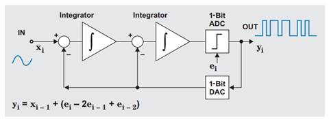
Figure 1. Ideal Delta-Sigma Modulator[1]
Mathematical calculations and simulations were performed using MATLAB's Delta-Sigma toolbox. The results of these calculations showed that a single bit second-order delta-sigma modulator with an OSR (Over-Sampling-Ratio) of 128 could achieve an SNR of around 90 dB; that is 20dB over our constraint of 70dB.
II. Digital Decimation Filter:
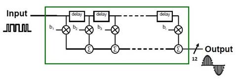
Figure 2. Ideal FIR Filter[1]
To filter out the out-of-band noise of the modulator, a cascade of two FIR filter were used. Decimation was performed between the two stages to minimize the power consumption of the filters.
2. Circuit Implementation:
The delta-sigma modulator was designed using specter simulator and cadence schematic editor. The digital filter was designed using MATLAB FDA tool and Verilog language and it's schematic synthesizers.
I. Delta-sigma Modulator: (Implemented by Danial Mohammadi and Mehrdad Malekmohammadi)
The delta sigma modulator was implemented using two Switch-Cap integrators, a clocked comparator, and a one-bit DAC. The capacitors of the first integrator were sized to satisfy the thermal noise requirements.
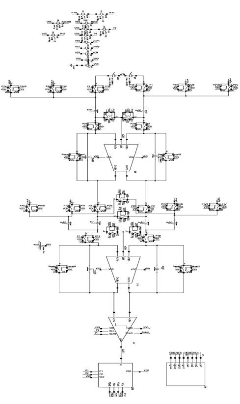
Figure 3. Delta-Sigma Modulator Schematic
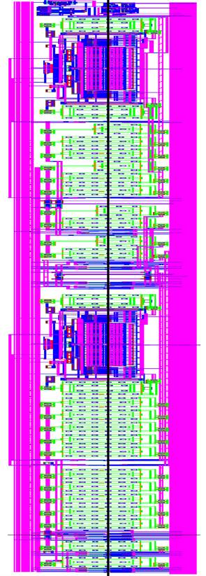
Figure 4. Delta-sigma Modulator Layout (980um*50um)
II. OTA : (Danial Mohammadi)
A switch-cap integrator requires an OTA at its core. The following folded cascode OTA was designed with special attention to the settling time and power constraints.
Table 2. OTA Specifications
|
VDD |
1.2V |
|
Power |
300uW |
|
Gain |
43dB |
|
Bandwidth |
250MHz |
|
Output Swing |
700mV (single ended) |
|
Phase Margin |
70 |
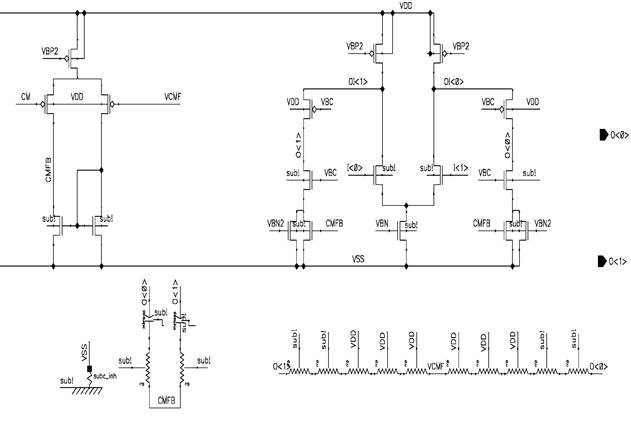
Figure 5. OTA Schematic
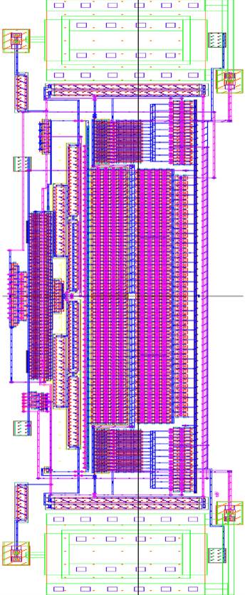
Figure 6. OTA layout ( 170um * 31um)
III. Comparator: (Saba Zargham)
A Strong-Arm comparator was implemented using 0.13um technology operating at a 6.4MHz clock frequency. The symmetricity of the layout is a crucial factor to avoid any offsets and hence has been taken into account during the design.
|
Clock |
6.4MHz |
|
Offset mean |
10u V |
|
Offset sigma |
2m V |
|
Hysteresis |
10u V |
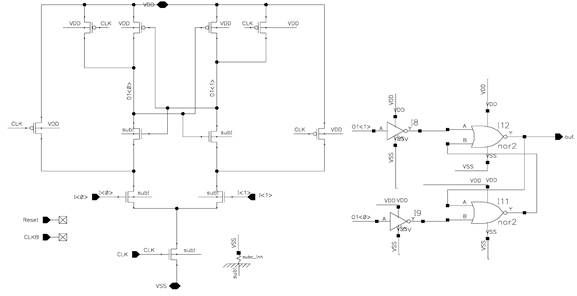
Figure 7. Comparator Schematic
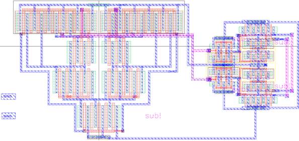
Figure 8. Comparator Layout (28um * 15um)
V. Switch: (Mehrdad Malekmohammadi)
Transmission gates were used as switches in order to benefit from their relative constant resistance. Moreover, a dummy transistor was introduced to deal with the clock feed-through phenomenon.
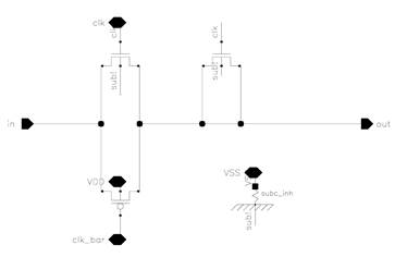
Figure 9. Switch Schematic
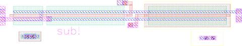
Figure 10.Switch layout
VI. 1-bit DAC : (Saba Zargham)
In this one-bit delta-sigma architecture the feedback is implemented by manipulating the switch-cap circuitry and how it adds and subtracts charges. Hence, the DAC in this circuit is not directly generating any voltages or currents, it only generates control voltages for switch-cap integrators.
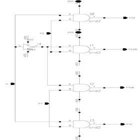
Figure 11. DAC Schematic
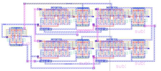
Figure 12. DAC layout ( 22um * 10um )
VII. Digital Filter : (Keivan Dabiri)
A cascade of two FIR filters were implemented in this design. There is a decimator immediately after each filter to bring down the overall output frequency of the system to 50KHz.
Table 3. FIR1
|
Stop Band Frequency |
200KHz |
|
Sampling Frequency |
6.4MHz |
|
Stop Band Attenuation |
40dB |
|
Order |
52 |
|
Power |
38.15uW |
Table 4. FIR2
|
Stop Band Frequency |
50KHz |
|
Sampling Frequency |
200KHz |
|
Stop Band Attenuation |
80dB |
|
Order |
19 |
|
Power |
37.47uW |
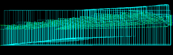
Figure 13. FIR1 Schematic
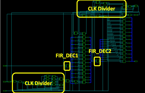
Figure 14. Digital Top-level Schematic

Figure 15. Filter1 Layout (1250um *25um)
![]()
Figure 16. Filter2 Layout (1800um *25um)
3. Simulation Results:
The simulation of this mixed-signal circuit was performed in two stages: Primarily, the simulation and verification of the analog delta-sigma modulator and afterwards, the verification of the digital filter. At first, a top-level delta-sigma modulator circuit was designed using ideal blocks ( ideal OTA, ideal comparator, etc.). This circuit was used to verify the mathematical calculation and also helped define specification of smaller blocks.
Moreover, each of the previously mentioned blocks was designed and tested separately using specter simulator. Eventually, these blocks were put together to verify their successful simultaneous operation as system.
The digital filters were designed and tested in MATLAB software. Later, the output of the specter simulator was imported into MATLAB in order to measure the in-bound and total SNR after the filtering performed by FIR1 and FIR2.
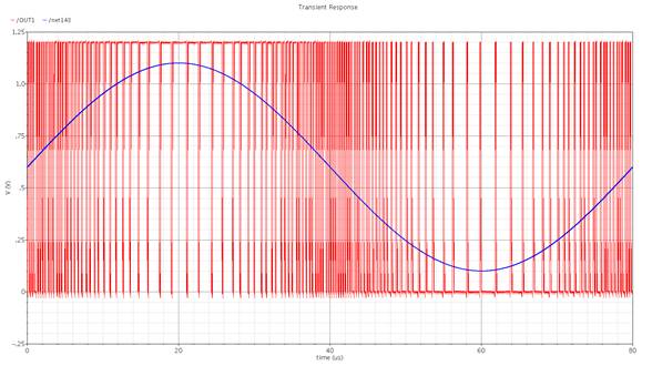
Figure 17.Transient simulation of fully transistorized delta-sigma modulator
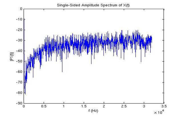
Figure 18. FFT of output of the delta sigma
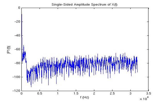
Figure 19. FFt of output of the filters
4. Chip:
The Path to the Library: "/nfs/ug/homes-0/m/moham400/CMRF8SF"
· Top-level design folder with pad frame= "ProjectFinal/TOP_LEVEl"
· Analog Top-level design without power pads (fully DRC and LVS clean)= "ProjectFinal/ANALOG_TOP_LEVEl"
· Delta_sigma modulator (fully DRC and LVS clean) = "ProjectFinal/ADC_main"
· Filter1(Generated by encounter)="final_filter1"
· Filter2(Generated by encounter )="final_filter2"
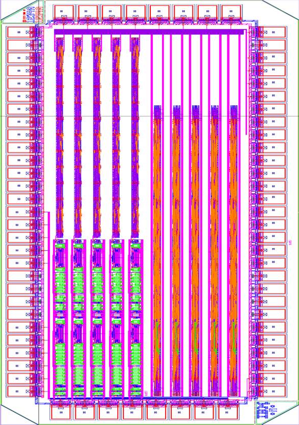
Figure 20. Chip Layout
5. LVS & DRC Report:
I. Top_level_Analog :
LVS
CELL COMPARISON RESULTS ( TOP LEVEL )
# ################### _ _
# # # * *
# # # CORRECT # |
# # # # \___/
# ###################
Warning: Unbalanced smashed mosfets were matched.
Warning: Ambiguity points were found and resolved arbitrarily.
LAYOUT CELL NAME: TOP_LEVEl_ANALOG
SOURCE CELL NAME: TOP_LEVEl_ANALOG
--------------------------------------------------------------------------------------------------------------
INITIAL NUMBERS OF OBJECTS
--------------------------
Layout Source Component Type
------ ------ --------------
Ports: 67 67
Nets: 487 487
Instances: 10975 11780 * MN (4 pins)
6820 8665 * MP (4 pins)
64 64 Q (3 pins)
130 70 * C (3 pins)
120 120 R (3 pins)
683 64 * D (2 pins)
487 201 * subc (2 pins)
------ ------
Total Inst: 19279 20964
NUMBERS OF OBJECTS AFTER TRANSFORMATION
---------------------------------------
Layout Source Component Type
------ ------ --------------
Ports: 67 67
Nets: 357 357
Instances: 240 240 MN (4 pins)
192 192 MP (4 pins)
64 64 Q (3 pins)
70 70 C (3 pins)
60 60 R (3 pins)
64 64 D (2 pins)
1 1 subc (2 pins)
20 20 SPDW_2_1 (4 pins)
55 55 _invb (6 pins)
20 20 _nand2b (7 pins)
10 10 _nor2b (7 pins)
11 11 _pmn2b (5 pins)
15 15 _pmn3b (6 pins)
10 10 _pup2v (4 pins)
20 20 _smn2b (5 pins)
------ ------
Total Inst: 852 852
DRC
--- RULECHECK RESULTS STATISTICS (BY CELL)
---
CELL pad_sig ............. TOTAL Result Count = 4 (256)
RULECHECK GRFY4 ...... TOTAL Result Count = 4 (256)
CELL ADC_main ............ TOTAL Result Count = 8 (40)
RULECHECK GR131_M2 ... TOTAL Result Count = 8 (40)
CELL TOP_LEVEl_ANALOG .... TOTAL Result Count = 22 (22)
RULECHECK GRLY6 ...... TOTAL Result Count = 10 (10)
RULECHECK GRE2 ....... TOTAL Result Count = 12 (12)
----------------------------------------------------------------------------------
--- SUMMARY
---
TOTAL CPU Time: 10
TOTAL REAL Time: 13
TOTAL Original Layer Geometries: 30951 (1694446)
TOTAL DRC RuleChecks Executed: 1618
TOTAL DRC Results Generated: 34 (318)
---------------------------------------------------------
II. Top_level:
LVS
CELL COMPARISON RESULTS ( TOP LEVEL )
# ################### _ _
# # # * *
# # # CORRECT # |
# # # # \___/
# ###################
Warning: Unbalanced smashed mosfets were matched.
Warning: Ambiguity points were found and resolved arbitrarily.
LAYOUT CELL NAME: TOP_LEVEl
SOURCE CELL NAME: TOP_LEVEl
--------------------------------------------------------------------------------------------------------------
INITIAL NUMBERS OF OBJECTS
--------------------------
Layout Source Component Type
------ ------ --------------
Ports: 67 67
Nets: 487 487
Instances: 10975 11780 * MN (4 pins)
6820 8665 * MP (4 pins)
64 64 Q (3 pins)
130 70 * C (3 pins)
120 120 R (3 pins)
683 64 * D (2 pins)
482 201 * subc (2 pins)
------ ------
Total Inst: 19274 20964
NUMBERS OF OBJECTS AFTER TRANSFORMATION
---------------------------------------
Layout Source Component Type
------ ------ --------------
Ports: 67 67
Nets: 357 357
Instances: 240 240 MN (4 pins)
192 192 MP (4 pins)
64 64 Q (3 pins)
70 70 C (3 pins)
60 60 R (3 pins)
64 64 D (2 pins)
1 1 subc (2 pins)
20 20 SPDW_2_1 (4 pins)
55 55 _invb (6 pins)
20 20 _nand2b (7 pins)
10 10 _nor2b (7 pins)
11 11 _pmn2b (5 pins)
15 15 _pmn3b (6 pins)
10 10 _pup2v (4 pins)
20 20 _smn2b (5 pins)
------ ------
Total Inst: 852 852
* = Number of objects in layout different from number in source.
References:
[1] T. I. Incorporated, "Analog, embedded processing, semiconductor company, Texas instruments," 1995. [Online]. Available: https://www.ti.com/. Accessed: Nov. 1, 2016.