TM3 Documentation

TM3 architecture
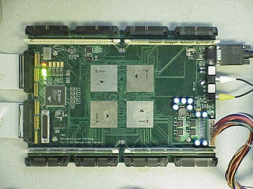
The TM3 contains four Xilinx virtex FPGA devices. Each of the four
virtex chips is connected to each of the other virtex chips with
a 98 bit bus. Each of these devices is also
connected to a synchronous sram, an io-connector, and a nibblebus that
allows communication with the housekeeping chip. The housekeeping chip
provides communication, download, and control functions through the
host computer. The housekeeping chip is not available to the user
outside of the built-in functions. Video in/out functions are
available on chip 3. The TM3 also has 4 independently programmable
clocks. Each chip receives the same 4 clocks. Schematics are available
to try to answer some of the details.
Top level
vnode (virtex fpga subsection)
Power supply
Video subsection
Clocks
The TM3 contains 4 clock PLLs, allowing the user to specify a clock
rate between 391KHz and 100MHz. While the PLL is rated only to 100MHz,
it appears to function correctly up to 130MHz. Use this upper band at
your own risk! Each of the four clocks, even if specified with the same
frequency, is phase independent. The SRAM clocks are always taken from
clk0. The nibblebus clock currently also uses clk0, but this could be
changed (with some pain) if really needed. Contact me about this.
The command for changing clock frequencies is:
% tm3 set_clk CLK_NO FREQ
where CLK_NO is the clock number from 0 to 3
and FREQ is frequency in hertz
Memory
Each of the four virtex chips has a synchronous
SRAM module connected.
This module is 512K x 64 bits, but due to a design fault, only 256K x 64 bits is
available. These SRAMs share the same pins with the video on fpga 3
and the general I/O connectors. Pick one and only one. The sram modules
are rated for clock speeds up to 50MHz, but the appear to function
well at significantly higher speeds. (They're made with 117MHz devices).
Test for yourself and judge the reliability at higher speeds. To use
an SRAM bank it must be first enabled using the command line instruction
% tm3 enable_sram CHIP_NO
where CHIP_NO is the fpga number from 0 to 3.
Video
Video input and outputs devices are connected to fpga-3. These devices
share the io pins with the SRAM and general io-connector, so you can only
use video OR sram OR I/O. If a video design requires memory, it must
use memory on a different chip. The video devices available are:
a NTSC video decoder, a
video RAMDAC for the digital to RGB out
conversion (VGA) and a NTSC encoder (this function still untested).
There is a video enable line on the TM3 that prevents these devices
from fighting with the SRAMs connected to the same chip. This line
is enabled with the command line instruction:
%tm3 enable_video
I/O
Each of the 4 Virtex FPGAs have 64 bits of general purpose I/O
connections available. These connections are realized through
2 40-pin headers adjacent to the appropriate FPGA. Each connector
has 32 data pins and 8 grounds. To determine the I/O connections,
one first has to examine the pinouts of the CONNECTOR.
These pinouts are then MAPPED to a bus
called io(31:0) which are in turn mapped
to the actual fpga connections as tm3_io_x[63:0].
WARNING: the I/Os on the TM3 with V1000s is 5v tolerant, but the
TM3 with V2000Es is only 3.3v tolerant!!!!!
If you must
connect 5v signals, they MUST be put through a 100 ohm
series resistor first.
Making things connect
Connecting your design to clocks, video, sram, and IO is done
automatically by just referring to the appropriate net name inside
your design. The TM3 router (gr) will do the rest. The net names
are predefined and listed in the tm3 boilerplate file. If you
want to rename nets, or change their port direction (io/out/inout),
you can make a local copy of this file in your design directory
and make the appropriate changes. Make a local copy of the boilerplate
file on the command line with:
% tm3boilerplate > tm3.boilerplate
The line format of the boilerplate file is as follows:
netname direction chip_no pin_no.
The netname is obvious. The direction field is not what you would expect.
It is defined from the standpoint of the described device. IE, tm3_clk_0_v0
out ..... means the clk has an output, which is an input on the FPGA. Only change direction on the tm3_io.... fields, the others are hardwired by their nature.
The chip_no field is obvious, chip 0 to 3, but there is also a chip 4. This
indicates a generic net name. It will connect to the appropriate net on
the device which refers to it. IE, "tm3_io_v31 inout 4 31" means that
referring to tm3_io_v31 on chip 3 will connect it to tm3_io_3_v31. This
can help to make designs portable between chips without changing net names.
Never change the last field. This defines where the net gets connected
to the FPGA. Another note on the net names within the boilerplate. These
nets use a slightly different name format than in VHDL. In VHDL, refer
to tm3_io[63 downto 0] to connect to tm3_io_v63 .... tm3_io_v0.
To connect nets between chips, just create pins on both chips
with the same name, and the router will make the appropriate connections.
Design entry
Creating and running designs is described HERE.
There are two supported ways of design entry, through VHDL and
tmcc.
%tm3vhd design0.vhd design1.vhd tm3_blank design3.vhd
% tm3xnf design0.xnf design1.xnf tm3_blank design3.xnf
This puts design0 in chip 0, design1 in chip 1, a null design in chip 2,
and design3 in chip3.
The tm3_blank keyword is used to force a null design into a device
if you want to force a design to reside on a later chip. You may
want to do this to force video circuits to reside on the chip they
are connected to.
An example of a tmcc implementation can be found HERE.
An example of a VHDL implementation can be found HERE.
Documentation of the ports package can be found HERE.
Documentation of tm3mon can be found HERE.
Note: There are some issues in the way the global router parses the entity declarations in VHDL. Only one port can be declared on each line, and the first port declaration must be on its own line, not the same line as "entity blah is port(" . Additionaly, the logic type of entity ports must be std_logic or std_logic_vector.
Running your design
simply enter the command
% tm3run
in your design directory
NOTE: your design directory must be world readable
Software
All the required software for the TM3 is located in ~tm3/bin. Example
applications are located in ~tm3/examples. These examples are the best
way to familurize yourself with the design flow of the TM3.
Debugging
There are a number of ways to debug your TM3 design. You can use the "ports"
package, jtag chain, or connect design signals to the I/O port and examine
them with a logic analyzer.
To use the jtag features of the TM3, use the command
% tm3 list_jtag
To group signals into buses, use the command
% tm3 list_jtag | tm3vars
