Memory Lab Simulation Software Guide
This guide briefly explains how to use the software program that you will be
using to complete the Memory Lab. The program simulates the operation of the
SRAM memory device that is located on the DE2 board, and allows you to observe
the results of your actions in real time. It only simulates the first 16
memory locations out of the 256 available on the SRAM chip.
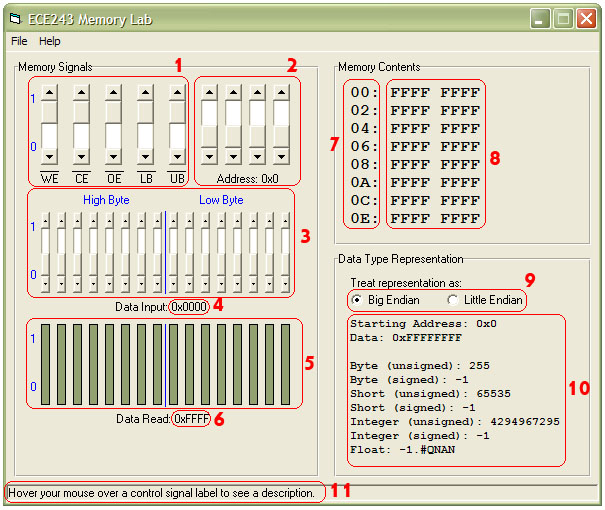
Figure 1: A sample screenshot from the Memory Lab program
Program Elements Description
- These are the control signal sliders. Any one of the control signals can
be changed at any time. If the CE (Chip Enable) signal is asserted, changes
to any other input signals will produce immediate results. The control signals
are active-low, and therefore they all begin in the high position initially.
For more information about the control signals, consult the device datasheet.
- These are the address signals. Using these 4 sliders, you can input 16
different addresses. Each address defines a memory location. For more information
about the specific nature of each memory location, consult the device datasheet.
As you move the sliders, the equivalent address will be displayed in hexadecimal
notation in the "Address" field under the sliders.
- These are the input data signals. They are connected to the 16 data lines
of the memory device, and represent the data to be written in the next write
operation. These signals are ignored during read operations.
- This field changes as the input data signal sliders are moved, and shows
the data to be written in the next write operation in hexadecimal format.
Double-clicking on this field will open a dialog box that allows entering
the data as a hexadecimal value, as an alternative to moving the 16 data input
sliders.
- These bars represent the output data that was read from the memory device
in the most recent read operation. The data represented by the bars remains
unchanged until the next read operation; therefore, you can think of them as
displaying the contents of a register that is connected to the 16 data lines
of the memory device, and is enabled only during read operations.
- This field displays the data from the last read operation (represented by
the bars above it), in hexadecimal format. Double-clicking on this field
will copy its contents to the data input field and change the position of the
16 sliders accordingly. It can be used to copy data from one memory location
to another.
- This vertical column displays the addresses of the memory contents panel.
They are in hexadecimal format, and each row contains two memory locations
(hence they increase by 2 each time).
- This portion of the memory contents panel displays the actual contents of
all the 16 memory locations. On each row, the leftmost column refers to the
address displayed on its left, and the rightmost column refers to the address
immediately following it. All displayed data is in hexadecimal format.
- This section of the data representation panel allows you to select whether
to interpret data (starting from the "starting address") as big endian or
little endian. For a particular "starting address", the word at that address
and the one immediately following it (if there is one) are read. The endianness
choice determines which one represents the high word, and which one represents
the low word.
- This field shows how the data read from the specified address is interpreted,
depending on the particular data type in question. To select an address, simply
change the address signals (but make sure that the CE signal is high to prevent
changes from being made). The endianness selection above determines the order of
the data that was read. Selecting the last address only displays data types that
use one word, because two words are not available.
- This is the status bar. Hovering your mouse over many of the labels and some
of the controls in the program will cause the status bar to display some extra
information about them.
Notes
- Be aware that closing the program will cause you to lose any changes that
you have made.
- To speed up the input of data, you can directly enter hexadecimal numbers
instead of moving the 16 sliders by following the suggestion in point 4 above.
- The program tries to immitate the behaviour of the SRAM memory device as
close as possible, by implementing the truth table that can be found on page 2
of the device datasheet. However, differences between the software simulation
and the actual hardware memory device may exist, especially due to the
non-deterministic electric effects to which hardware is prone.
Good luck!