P. Chow and J. Rose
Fall 1996
The circuit you are to build is not really complicated in its function, but because of the low-grade technology you will be using to build the circuit, you will require a large number of parts. This will model the task of building large circuit systems. Some amount of planning and care is required on your part to design and build the circuit in a way that will allow you to easily understand and debug it.
WARNING: This lab will require significant preparation time and will be the most challenging in terms of its complexity and the time it will require. You are encouraged to work with others to discuss the design and divide up the chore of entering the schematics.
Proper circuit building and testing procedures in the lab are the ONLY way that you will be able to complete the lab satisfactorily in the given time. The extensive writeup below was not written to be ignored! Do so at your own risk!!!
This section describes the function of the circuit and specifies how it is to be implemented.
The required structure is shown in the block diagram of Figure 1. It consists of two level-sensitive registers, B and C, as well as an adder. In general, inside a computer this would be an Arithmetic Logic Unit (ALU) which could also perform other functions such as subtraction, shifting, and logical functions.
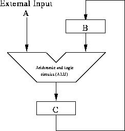
Figure 1: An ALU/Adder Configuration.
Consider first a simple addition operation involving operands at external Input A and in Register B. The sum of A+B is to be sent to Register C. The sequence of clocked events needed to accomplish this is as follows. The first operand is made available at A via the external input. At the same time Register B is cleared to contain all zeros. At this point the output of the ALU should be equal to the operand at A, which can now be loaded into Register C. Then, by transferring the contents of Register C to Register B you can, in effect, load the first operand into B. Next, the second operand is made available at A and the desired addition is performed, with the sum being loaded into Register C.
The relative timing of the signals Clock-B, Clock-C, and the inputs at A in this circuit are very important to the correct operation of the circuit. For example, the data must be available at the input to the latches, before the latches are clocked. This defines the timing constraints of the circuit.
Design, construct and test a complete 2-bit version of the circuit in Figure 1. Use toggle switches to provide the input at A. Build the registers B and C using NOR gates (74LS02, 74LS27). To implement the necessary gating and control use AND gates (74LS09, 74LS11), NAND gates (74LS00, 74LS10), and inverters (74LS04). Use the pulse switch to manually provide single clock pulses. You must be careful to control the gating of the clock (perhaps using one of the toggle switches) in such a way that the contents of Register B do not propagate to C and back to B within the same clock pulse. The adder (which you studied in LogicWorks Exercise #1) may be implemented with EX-OR gates (74LS86) and other gates as necessary.
This section describes all of the work that must be done before starting to build any hardware.
If you are not clear about the operation of the above circuit, try some examples with pencil and paper to see how the data flows around the circuit. This part of the circuit is often called the datapath because it is the path that the data takes. Then try to understand the timing of the data flow, i.e., when you will need to clock the various registers. This is the control part of the circuit. In this lab, the control is done by switches. We will not be building logic circuits to implement the control.
This part is primarily sketching out the circuit design using pencil and paper. You will later take this design and create a set of schematics using LogicWorks.
Start by drawing a high-level diagram showing the inputs and outputs to the system you are building. In this case it will be a single box, with the signals going into and out of it labelled.
The next step is to partition the problem into major subsections, again showing the inputs and outputs, but now also labelling the signals flowing between the subsections. Start with Figure 1, but you will need to add a bit more detail to show all of the signals. Call this the Level 3 circuit diagram, and the blocks in it, the Level 3 blocks. You will also need to specify the timing of the input and output signals to and from each block. This could be done by means of a timing diagram showing the clock signals used for the registers and when the other signals must be stable in relation to the clock.
With this partitioning done, you can now look at the partitions, or Level 3 blocks, individually. As long as you meet the timing constraints specified above, you can design these blocks independent of how the rest of the circuit is designed. In larger projects, this partitioning can happen for several iterations, and as long as the specifications of the signals at the partitions are obeyed, the design of the circuits in each partition can happen in parallel, i.e., several designers can work on different parts of the design at the same time. In this case, draw the circuits at the next lower representation by showing the registers as being composed of individual latches (drawn as boxes still), and the adder as being composed of full adder blocks. Do not forget to carefully label and give timing information for all signals, including those between the blocks. These are the Level 2 circuits, containing Level 2 blocks. Note that you still have not drawn any gates.
You should now be at the lowest level where you will have to design the circuits. In this case they are the latch blocks and the full adder blocks. Give the circuit designs for the individual blocks. Call these the Level 1 circuit diagrams, where the Level 1 blocks are really the gates.
You are now done with the basic circuit design. The next task is to verify that your logic design works.
Using LogicWorks, create drawings of your Level 1 circuits. Simulate them and verify that they are working properly. You have to make a choice about the parts library to use, and to do this you should consider the implementation technology. You will be using 7400 series parts.
What are your possible library choices?
What are the pros and cons of each choice?
Since your Level 1 circuits are basic building blocks, they are going to be used a number of times in the final circuit. It is desirable to create a simpler symbol for these circuits. Consult the Logicworks 3.0 manual, Chapter 11 (on the Device Editor) and pages 149-158 concerning the design of sub-circuits. These tell you how to create a symbol for the Level 1 circuits. This need only be a box with the appropriate inputs and outputs, with some sort of label.
Hint: Often, when trying to learn a new feature of a CAD tool, it is best to try using a very simple example before working with your actual circuit. Even after this, the really paranoid would make a backup copy of their work to date, in case they misuse the feature and do irreparable damage.
Once you have symbols for your Level 1 circuits, you can move up to your Level 2 circuits. Create your Level 2 schematics using the symbols you have created for your Level 1 circuits. Again, you may find it convenient to create symbols for your Level 2 circuits. You should also simulate your circuits at this level.
This process is repeated until you get to the top level, which is Level 3 in this case. Your top level schematic should look a lot like Figure 1. A final set of simulations should be done to confirm that your complete circuit works.
Note: At each step, we simulate the schematics that we have created so far. Doing this means that we have confidence that the work done so far is correct so that when we create more complex schematics, we should not have to worry about the subcircuits not working. Simulation is a means of design verification.
The approach you have taken for creating your schematics is a modular approach that follows the hierarchical decomposition you used for the initial design. Building and testing the schematics in this way helps you to have confidence that the full system will be correct.
Once you have a set of schematics that simulate correctly, you know that your circuit is functionally correct. There are still many other issues that must be considered in complex circuit systems, with timing and power consumption being the most critical. For very high speed systems, an analysis of the electromagnetic properties is required to find out if there are problems such as crosstalk interference between signals on the board, and whether the board will interfere with the operation of your TV.
The next step is to map the full design into the technology that you have chosen, or been given. In this case, you should use the selection of gates that were specified previously in Section 2.2. For each gate in your design, you must assign chip and pin numbers. If a block in your schematic is actually a subcircuit, then you assign it a drawing number, which corresponds to a copy of the subcircuit schematic. For example, each block in your Level 2 schematic that represents a latch should have a corresponding copy of the Level 1 schematic with the pins and chips assigned.
When you are done, you should have a set of schematic drawings that could be given to anyone with some knowledge about building circuits. With possibly some additional descriptions about how the circuits operate this person should be able to implement your design.
The design approach that has been described here is called a top-down design approach: start from the highest level, and reduce the problem to smaller and smaller pieces. A bottom-up approach starts at the opposite end: start designing circuits right away. In reality you will find that neither approach is strictly correct, and that you will have to do a bit of both to get the best solution: start from the high-level but keep in mind that choices for implementation at the low level can influence your decisions about possible tradeoffs at the high level. For example, the design of a lawn mower would look very different depending on whether you were going to use a spinning blade or a goat to actually do the cutting of the grass.
Do not confuse top-down design with the implementation process. When you build your schematics for simulation, and when you build your circuits, you do this bottom up. Obviously, when doing an implementation, be it a simulation, or hardware, you start from the basic components.
The recommended procedure for building your circuit and suggestions for debugging it are outlined in this section.
Consider the connections between the Level 2 blocks that you need, and decide on a reasonable positioning of the chips to minimize the lengths of the wires.
Construct the Level 2 blocks using the Level 1 schematics, but do not connect them to any other Level 2 blocks. Test each of the Level 2 blocks individually to make sure they function properly in isolation.
Once you have the Level 2 blocks working, connect them together to form the Level 3 blocks. Test that the Level 3 blocks are working correctly. You should now have a working adder block and two working register blocks.
Finally, connect the Level 3 blocks to form the Level 3 circuit. This should be the final circuit. Assuming that you have connected the Level 2 blocks correctly, and that you have not broken anything while doing this, the full circuit should work. Test and demonstrate to a TA that your circuit is working.
The approach you have used to build your circuit is a modular approach whereby you test the pieces as you put them together, much like you did with your schematics. The idea is to make sure the circuit works as you construct it, making the final integration easier. In theory, if you have correctly specified the interfaces, and have strictly adhered to the interface specifications, then the full circuit should work the first time!
Now that you have a working circuit, give the schematics to the TA, turn your backs, and wait while the TA modifies your wiring.
The scenario is now this: You are faced with a circuit that does not work, and your boss wants it fixed ASAP. You may or may not be given symptoms of the incorrect circuit behaviour. Be prepared to explain to the TA what you are doing as you go, or what you did if the TA comes back later.
The first step is to figure out what the circuit is doing or not doing. There are two ways to do this: by guessing and by being methodical.
After observing the behaviour of the circuit, you might first try a few intelligent guesses and see if you get lucky. Do this by postulating a problem that could produce the observed behaviour, and then verifying that it is indeed the problem. You get better at this only by experience. Sometimes this type of debugging includes the use of the simulator. In this case, you try to reproduce the observed incorrect behaviour by introducing possible circuit bugs into your schematic. When your schematic behaves incorrectly in the same way as your circuit, then you have probably found the problem.
If guessing doesn't get you anywhere, then you will need a more methodical approach. Start at the inputs and trace the flow of the data through the circuit. In this case, see if you can clear Register B. If that works, apply inputs at Input A, and see if the adder works. Carry on in this manner until something stops working. You may then wish to isolate the part that isn't working by removing some wires, and then look at it in more detail by trying to isolate the problem down to smaller subcomponents. Removing wires isn't always an option, and this can complicate the debugging process. You should observe that this is an iterative approach much like you did when starting with the high-level specification and then reducing it to the individual gates. Using a similar process when debugging will eventually get you to the part where the problem lies.
If you exclude electrical and noise problems, debugging hardware, and debugging a simulation are much the same.
Once you have completed, you should do a review of your design procedure. Some possible questions to ask yourself, and your design team:
A complete working schematic and simulation, as described in Section 3, are required for the preparation.