P. Chow and J. Rose
Fall 1996
NOTE: You should demonstrate the final circuit in both parts to a TA.
The purpose of this experiment is to revisit the adder circuit that you built in Lab 3, but do it with the higher-density PAL chips.
Having constructed the 2-bit circuit in Lab 3, you have undoubtedly become aware of the wiring complexity that can be involved in logic circuits, and the care that must be taken when designing and constructing circuits with lots of chips. Consider now the possibility of extending your design to the 4-bit case. How many gates and wires would you need? The problem is simplified considerably if larger chips with more gates are used, i.e., chips that contain several basic gates interconnected internally to provide easy to use functional blocks. Examples might be 4-bit adder chips, which provide a specific MSI function, or PAL chips, which are more flexible.
In this lab you will design, construct, and test a complete 4-bit version of the circuit from Lab 3, using the P18CV8 PAL device. First, note that the PAL includes edge-triggered D flip flops. How are they different from the flip flops you designed for Lab 3?
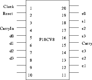
With the use of edge-triggered flip flops, the circuit only needs one register stage. Why? Figure 1 shows the circuit to build. It can be done in a single P18CV8. Details of the Adder and Register are shown in Figure 2. You should use the pinout shown in Figure 3.
Develop the ABEL equations for this circuit, program the PAL, and test. The following is an example of the kind of statements you will need:
s0 := d0 :+: s0 :+: carryin;
Note that because ![]() ,
, ![]() , and
, and ![]() will be on the left side of
some equations, you are required to assign them to output pins
even though you are not using them as outputs.
This rule is part of the ABEL language.
By looking at the diagram of the P18CV8 in the lab manual, can you
determine why this is necessary?
will be on the left side of
some equations, you are required to assign them to output pins
even though you are not using them as outputs.
This rule is part of the ABEL language.
By looking at the diagram of the P18CV8 in the lab manual, can you
determine why this is necessary?
For your test vectors, you should use the .c. constant to indicate the clocked input.
Preparation: Describe your design in ABEL-HDL, compile and simulate it using the abel program. Come to the lab ready to program and test a working PAL.
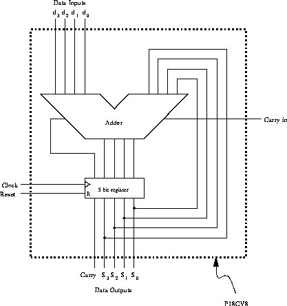
Figure 1: ALU configuration using edge-triggered flip flops.
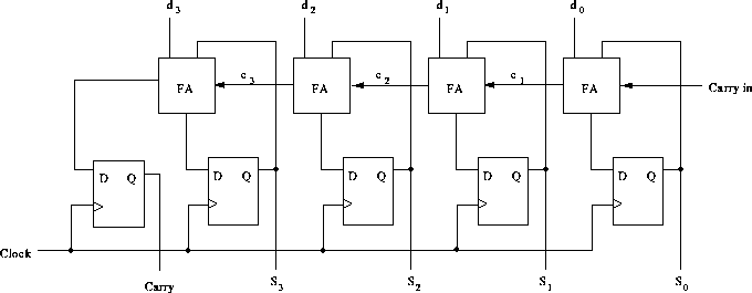
Figure 2: Details of the adder and register.
You will be given, during the lab period a word description of a synchronous sequential circuit to design with a PAL. This may be a counter or a finite state machine.