Most digital systems are composed of both logic and memory. Field-Programmable Gate Arrays (FPGAs) have traditionally been used to implement the logic portion of a system, leaving the memory to be implemented using standard off-the-shelf memory chips. As the capacities of FPGAs grow, however, it becomes feasible to implement memory directly on the FPGA itself. This paper describes and compares a set of architectures for implementing on-chip Field-Configurable Memory (FCM).
There are several advantages to including memory on an FPGA. First, on-chip memory reduces the demand on the FPGA's I/O resources, especially for wide memories. Secondly, on-chip memory will likely result in faster circuits, since the I/O pins need not be driven which each access. Finally, on-chip memory will likely reduce a system's chip count, resulting in less expensive implementations.
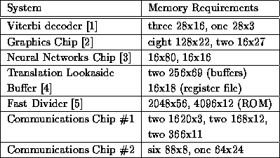
Table 1 gives several example systems and their memory requirements.
We will refer to the memory requirements of a given application circuit as a logical memory configuration. Each independent memory within a logical memory configuration will be referred to as a logical memory. Many configurations contain more than one logical memory; for example, the Viterbi decoder in Table 1 requires four logical memories. The specification of these four memories, with their widths, speeds, and any other special requirements (such as dual-port) make up the circuit's logical memory configuration.
The primary difference between standard memory and memory in FPGAs is that FPGA memory will be used in many different contexts and must, therefore, be flexible. Each circuit in Table 1 requires a different number of memories and different memory sizes. A good FCM architecture will allow the efficient implementation (in terms of area and speed) of a wide variety of logical memory configurations.
Since logic and memory have very different characteristics, we begin with the assumption that an FPGA that can implement both efficiently will have separate resources for each. It is well-known that look-up tables with about 4 inputs are well-suited for implementing logic [6]. A large memory, however, is implemented more efficiently using larger arrays; not only is the extra overhead of using many small look-up tables avoided, but also dedicated decoding and mapping circuitry can be provided instead of using logic blocks for that purpose. One of the questions we set out to answer in Section 4 is how big each of these blocks should be. In the architecture presented in Section 2, the data width of each block is configurable; the appropriate amount of configurability in each block will also be examined in Section 4.
FPGA architectures containing both logic blocks and memory arrays can be classified into two categories: centralized and distributed. In a centralized architecture, the memory arrays are all grouped together on the FPGA, which allows dedicated circuitry for combining these blocks to be easily included. In a distributed architecture, memory arrays are distributed throughout the chip. A distributed architecture should work well for applications that don't need to combine arrays to form large memories, since it would likely be easier to place the memories closer to their address and data sources and sinks. In this paper, we restrict our discussion to centralized architectures.
Several FPGA vendors already offer limited memory capability [7, 8, 9, 10, 11, 12]. For the most part, these existing architectures are aimed at implementing circuits with relatively small memory requirements. For circuits with larger memories, new architectures are needed. In the next section, we present a family of centralized Field-Configurable Memory architectures that can be included in an FPGA. Since little work has been done in this area, it is unclear how such architectures should be compared and evaluated. Section 3 describes our approach, and Section 4 examines the effects of changing various parameters of the architecture.