This section describes a family of Field-Configurable Memory architectures similar to the FiRM FCM described in [13]. The FCM architecture, illustrated in Figure 1, consists of b bits divided evenly among n arrays that can be combined (using the address and data mapping blocks) to implement logical memory configurations. The parameters used to characterize each member of this architectural family are given in Table 2. Since each logical memory requires at least one array, one address bus, and one data bus, the maximum number of logical memories that can be implemented on this architecture is the minimum of m, r, and n.
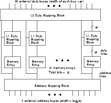
Figure 1: General architecture for a centralized FCM
Table 2: Architectural Parameters
Flexibility is achieved by this architecture in two ways: by allowing the user to configure the effective output width of each array, and by allowing the user to combine arrays to implement larger memories. First consider the effective output width of each array.
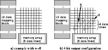
Figure 2: L1 data mapping block
Each array has a nominal width of w and depth of ![]() . This
nominal aspect ratio can be altered by the level 1 (L1) data mapping block.
Figure 2(a) shows an example L1 data mapping block in which
w=8. Each dot represents a pass-transistor switch. In this example, the
set of allowable effective output widths,
. This
nominal aspect ratio can be altered by the level 1 (L1) data mapping block.
Figure 2(a) shows an example L1 data mapping block in which
w=8. Each dot represents a pass-transistor switch. In this example, the
set of allowable effective output widths, ![]() , is
, is ![]() ,
meaning each array can be configured to be one of
,
meaning each array can be configured to be one of ![]() x1,
x1,
![]() x2,
x2, ![]() x4, or
x4, or ![]() x8.
Figure 4(b) shows two sets of switches, A and B,
that are used to implement the
x8.
Figure 4(b) shows two sets of switches, A and B,
that are used to implement the ![]() x4 configuration. One of the
memory address bits is used to determine which set of switches, A or B,
is turned on. Each set of switches connects a different portion of the
memory array to the bottom four data lines.
x4 configuration. One of the
memory address bits is used to determine which set of switches, A or B,
is turned on. Each set of switches connects a different portion of the
memory array to the bottom four data lines.
Notice that the mapping block need not be capable of implementing all power-of-two widths between 1 and w. By removing every second switch along the bottom row of the block in Figure 2(a), a faster and smaller mapping block could be obtained. The resulting mapping block would only be able to provide an effective data width of 2, 4, or 8, however, meaning that the resulting architecture would be less flexible. Section 4 examines the impact of removing L1 data mapping block switches on area, speed, and flexibility.
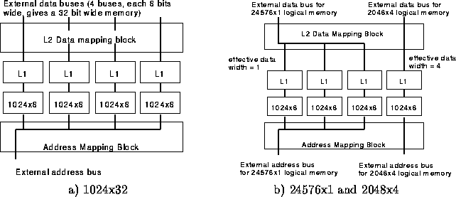
Memory flexibility is also obtained by allowing the user to combine arrays to implement larger memories. Figure 3(a) shows how four 1024x8 arrays can be combined to implement a 1024x32 logical memory.
Figure 3: Two example mappings
In this case, a single external address bus is connected to each array, while the data bus from each array is connected to separate external data buses (giving a 32-bit data width). Each L1 data mapping block connects 8 array data lines directly to the 8 L1 outputs.
Figure 3(b) shows how this architecture can be used to implement a configuration containing two logical memories: one 24576x1 and one 2048x4. The three arrays implementing the 24576x1 memory are each configured as 8192x1 using the L1 data mapping block, and each output data line is connected to a single external data line using bidirectional pass transistors. Two address bits control the pass transistors; the value of these address bits determine which array drives (or is driven by) the external data line. The 2048x4 memory can be implemented using the remaining array, with the L1 block configured in the ``by 4'' mode.
The topology of the switches in the level 2 (L2) data mapping block
and the address mapping block determine to what extent the arrays can
be combined. If both of these mapping blocks are fully populated, meaning
any external bus (both address and data) can be connected to any array,
a very flexible, but slow, architecture would result.
As a compromise between speed and flexibility, the switch
topologies in Figure 4 will be used in this paper.
In this figure, each dot represents a set of switches controlled by
a single programming bit, one switch for each bit in the bus
(w in the L2 data mapping block and ![]() in the
address mapping block) [13].
in the
address mapping block) [13].
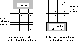
Figure 4: Level 2 data and address mapping block topology (n=m=r=4)
This topology can support almost all required mappings as long as the mapping algorithm is free to set the external bus and array assignments, but, because there are fewer switches than in a fully populated block, the delay is less than in the fully populated case. In Section 4, n will be varied; it is simple to extend the same basic pattern to an array of any width.
In addition to address and data lines, write enable signals are required for each array. The write enable lines can be switched in the L2 mapping block just as the data lines are. In order to correctly update arrays for effective widths less than the nominal width, we assume that the arrays are such that each column in the array can be selectively enabled. The address bits used to control the L1 mapping block can be used to select which array column(s) are updated.