We assume that an FPGA with embedded memory consists of distinct logic and memory resources, as illustrated in Figure 1. The memory resources consist of a set of identical arrays that can be combined to implement the required user memory configuration, similar to [6]. The number of bits in each array is fixed, but the aspect ratio can be configured by the user. In the results presented in Section 4, we have assumed that each array has two kilobits, and has a configurable data width of 1, 2, 4, or 8 (similar to [2] and [7]). Unlike [6], here we assume that each memory array has separate input and output data ports (as well as an address port).
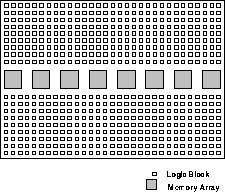
Figure 1: FPGA with Embedded Memory
The logic resources of the FPGA are assumed to consist of five-input lookup
tables, interconnected using symmetric horizontal and vertical channels like
those of [1] and [4]. At the intersection of
each horizontal and vertical channel is a switch block. The flexibility of
each switch block, ![]() , is defined as the total number of possible
connections offered to each incoming wire [1]. In this paper,
we assume
, is defined as the total number of possible
connections offered to each incoming wire [1]. In this paper,
we assume ![]() , which is consistent with previous work. All segments are
of length 1; that is, segments only connect neighbouring switch blocks.
Each pin of each lookup table can be connected to two channels; within each
channel, each pin can be connected to
, which is consistent with previous work. All segments are
of length 1; that is, segments only connect neighbouring switch blocks.
Each pin of each lookup table can be connected to two channels; within each
channel, each pin can be connected to ![]() tracks. In
Section 4, we vary
tracks. In
Section 4, we vary ![]() between W and
between W and ![]() ,
where W is the number of routing tracks per channel.
,
where W is the number of routing tracks per channel.
The memory arrays are assumed to be positioned in a single row in the middle of the chip, as shown in Figure 1, with logic blocks above and below the memory arrays. This is similar to the Altera FLEX10K architecture [2] and the Actel 3200DX architecture [3].
Figure 2 shows the assumed interconnect structure between the logic and memory portions of the FPGA. In the figure, each solid line is a channel of W parallel routing tracks. The vertical tracks in the top half of the logic are connected to those in the bottom half, and the pins on each memory array are connected to one or more of these vertical tracks. Note that in Figure 2, the vertical tracks are shown to ``bend'' around the memory blocks; in multi-metal layer implementations, the vertical tracks might simply cross on top of the arrays.
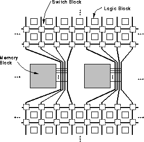
Figure 2: Memory/Logic Routing Structures
We define the flexibility of the memory/logic interconnect, ![]() , as the
number of vertical tracks to which each memory pin can connect. If there
are r logic blocks per memory block in the horizontal dimension, the
maximum possible
, as the
number of vertical tracks to which each memory pin can connect. If there
are r logic blocks per memory block in the horizontal dimension, the
maximum possible ![]() is rW (in Figure 2, r=4). In
Section 4, we will vary
is rW (in Figure 2, r=4). In
Section 4, we will vary ![]() from 1 to its maximum
value and examine the effects on routability and delay.
from 1 to its maximum
value and examine the effects on routability and delay.