Please view our openings for up-to-date information
(Credit
for the work highlighted here goes to our entire team of very talented current and
past graduate students and postdoctoral fellows!)
Research
goal
The main goal of our research program is to help
maintain and improve health by providing medical doctors, biomedical
researchers and/or patients with novel
microelectronic technologies for miniature medical devices that directly or
indirectly interface with the human body in order to monitor its
function and, in some cases, influence it. We also target scientific,
industrial, consumer and environmental sensory electronics applications.
Motivation
Modern healthcare practices suggest that
patient-interfacing medical devices of the future are to be potent, ubiquitous,
and inexpensive. Our research investigates such medical devices. These devices
address specific unmet healthcare needs, particularly those in medical monitoring, diagnostics and therapy
in clinics, biomedical research labs and at home. Of our immediate interest are
applications in neuroscience and molecular biology.
We target disorders and diseases with limited conventional treatment options or
with costly diagnostics options. Specific medical applications include
electronic therapy for intractable epilepsy [J21, C51, C56, J13] and electronic screening
for early detection of certain types of cancer [C45, C50, J16, J27, J28, J11, J15, J24].
Approach
Interfacing with the human body for the purpose of
maintaining or improving health requires a variety of sensory functionalities.
These can be as simple as monitoring key vital signs, or as complex as
monitoring electrochemical activity of the brain or examining biochemical
content of bodily fluids. In our research we target applications
where novel implantable, wearable or disposable biomedical devices with complex
sensory functions are uniquely enabled by low-cost integrated circuit (IC)
technologies such as CMOS.
Specifically, we focus on the design of integrated
circuits, VLSI architectures and signal-processing algorithms that comprise the
core of a sensory medical device. Such
sensory devices not only acquire raw sensory data, but also perform local
sensory signal processing (such as feature extraction and machine learning data
classification algorithms), and provide feedback information or, in some cases,
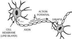
feedback action as shown in Figure 1. One successful example of such a system
is a single-chip brain implant for treatment of intractable epilepsy we
developed that accurately detects early seizures and automatically triggers
neuro-stimulation to effectively control them [J21, C51, C56].
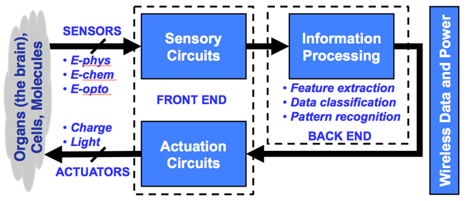
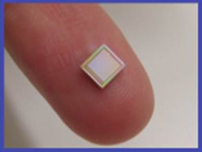
Figure 1. Functional block diagram of a biomedical
sensory microsystem (left) and an illustration of its form factor (right).
Key
challenges / RESEARCH DIRECTIONS
1. Sensor/Actuator Fabrication and
Microsystem Integration
From the sensor/actuator
fabrication and microsystem integration perspective, for potency,
ubiquity and low cost it is often advantageous to utilize sensory properties of
either the integrated circuits themselves or of additional small sensors with a
similar form factor. This approach avoids bulky externally connected sensors or
associated packaging costs. In our previous work, we have demonstrated
suitability of silicon integrated
circuits (ICs) to be further (post-CMOS)
integrated with various arrays of on-die and off-die sensors for
implantable, wearable and disposable microsystems implementations.
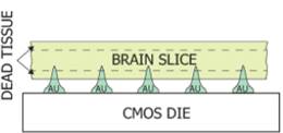
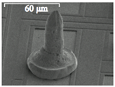
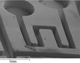
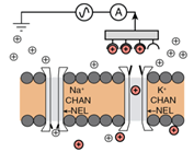
1.1 In electrophysiological sensing/actuation
applications, we have developed various such prototypes
including: arrays of gold micro-needles to monitor spatial maps of electrical
neural activity in the brain for in vitro epileptic seizure propagation studies
[J9,
C27, J26, J7,
J12, J25] (Fig. 2a, with Prof. Peter
Carlen), active neural probes comprised of 2D arrays of platinum micro-needles
directly co-integrated with neural amplifiers on an integrated circuit (Fig.
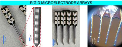
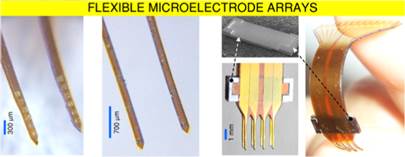
2b, with Prof. Peter Carlen), and 3D arrays of both rigid and flexible
microelectrodes for in vivo implantation (Fig. 2c, with Prof. Raafat Mansour
and Dr. Salam Gabran).
(a)
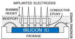
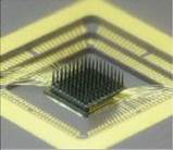
(b)
(c)
Figure 2. Examples of sensor fabrication and
microsystem integration techniques for electrophysiological
sensing/actuation applications.
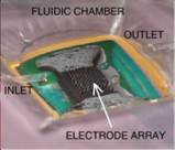
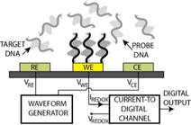
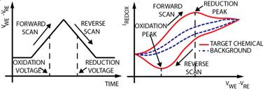
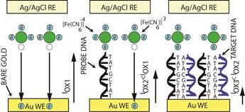
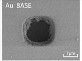
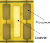
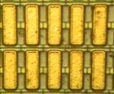
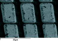
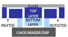
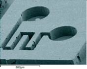
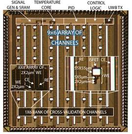
1.2 In electrochemical sensing/actuation
applications, the sensors prototyped by us range from arrays of
flat gold microelectrodes accessed by on-chip microfluidic structures (Fig. 3a,
with Prof. Guenther), to nanostructured gold electrodes with affinity-based
chemical functionalization (Fig. 3b; with Profs. Ted Sargent and Shana Kelley),
to post-implantation fouling-resistant on-gold chemical coating (Fig. 3c, with
Profs. Peter Carlen and Michael Thompson). Applications include molecular
diagnostics such as measuring pathogen DNA concentration and cancer screening
(Fig. 3b) [C45, C50, J16, J27, J28] and measurement of
concentration of neurochemicals for brain neurochemistry studies and
diagnostics [J35, J17, C37, J5]
(Fig. 3c).
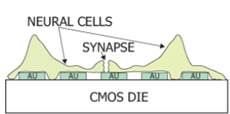
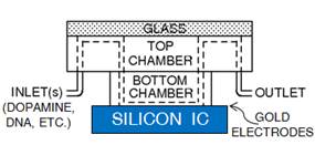
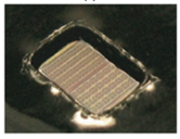
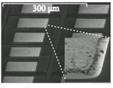
(a)
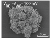
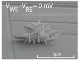
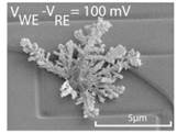
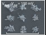
(b)
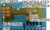
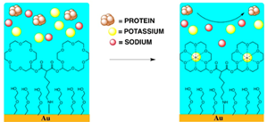
(c)
Figure 3. Examples of sensor fabrication and
microsystem integration techniques for electrochemical
sensing/actuation applications.
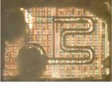
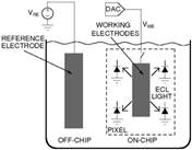
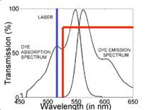
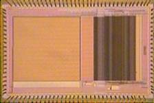
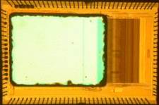
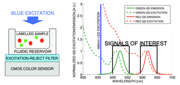
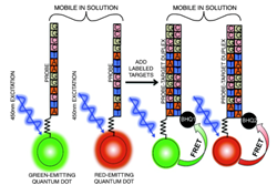
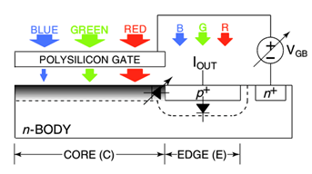
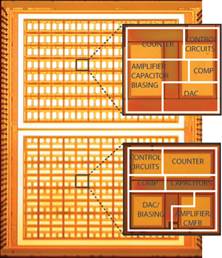
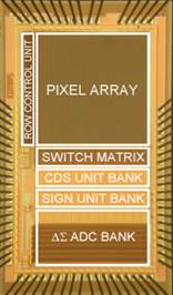
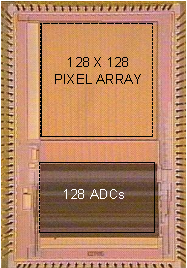
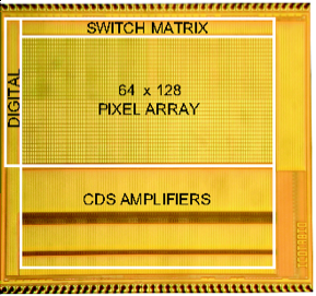
1.3 In electro-optical sensing/actuation
applications, we have
prototyped various CMOS imager sensors for both conventional non-contact and
emerging contact imaging applications. These include photo-detector arrays for
electro-chemi-luminescence (ECL) excitation and sensing (Fig. 4a) with fluidic
samples delivered through microfluidic structures (Fig. 4b, with Prof. Axel
Guenther) as well as single-color (Fig. 4c, with Prof. Glenn Gulak) and
multi-color (Fig. 4d, with Prof. Ulli Krull) fluorescence contact imagers.
Applications range from pesticide detection (Figs. 4a and 4b) to optical
imaging of various micro-scale biological objects such as fluorescently labeled
DNA microarrays (Figs. 4c and 4d) [J11, J15, J18, J23, J24].
(a)

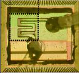
(b)
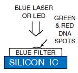
(c)
(d)
Figure 4. Examples of sensor fabrication and
microsystem integration techniques for electro-optical
sensing/actuation applications.
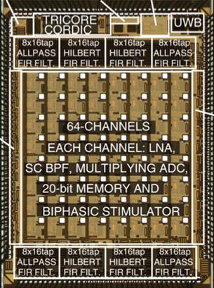
2. Front end: Sensory/Actuating
Circuits
From the front-end circuits perspective, the key
challenges are low signal-to-noise ratio, large sensory signal offset and
drift, high interference levels, intrinsic electronic noise, time-varying
signal source properties, various artifacts and numerous other sensory
interface-related issues. In our previous work, we have addressed these issues
individually by sensory transducer innovations
(e.g., novel photodetectors [J15,
J23]) and various integrated circuit design solutions (e.g.,
novel signal filtering circuits [J6, J20] and novel chopping circuits [J19, J23]). Our latest projects
include electro-physiological sensors for brain activity monitoring and
modulation (Fig. 5a), electro-chemical sensors for in vivo neurochemistry
monitoring and in situ molecular diagnostics (Fig. 5b), as well as optical
sensors for molecular detection, cellular imaging and computational photography
(Fig. 5c).
(a)
(b)
(c)
Figure 5. Examples of our sensory front-end
integrated circuits designs for (a) electro-physiological, (b) electro-chemical
and (c) opto-electronic sensory applications.
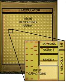
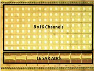
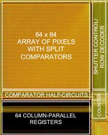
3. Back End: Computational Circuits
From the back-end circuits perspective, the key
challenges are the ever-growing requirements for intelligent ways to process
large amounts of sensory signal information (or big data), higher sensory data
processing throughput, and higher integration density with a limited power budget. The power budget is often constrained by heat
dissipation (such as that into the tissue surrounding an electronic implant).
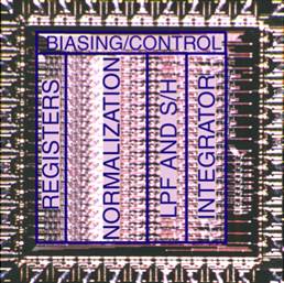
In our previous work, we have developed a number of circuit
design techniques that break the conflicting throughput-area-power trade-offs.
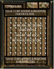
These include energy-efficient information-to-digital converter architectures
that perform computationally-expensive feature extraction and data
classification, such as in the application of triggering therapeutic
closed-loop neurostimulation (Fig. 6a) [J6,
J10,
J16, J20], and energy-efficient
mixed-signal VLSI architectures for accelerating machine learning in sensory
data classification applications (Fig. 6b, with Prof. Gert
Cauwenberghs) [J8,
J13, J14, J20]. Within this thrust, we are
currently pursuing research on energy-efficient digital and mixed-signal VLSI
accelerators for high-performance machine learning and artificial intelligence
applications and computing architectures co-integrated with sensory arrays.
(a)
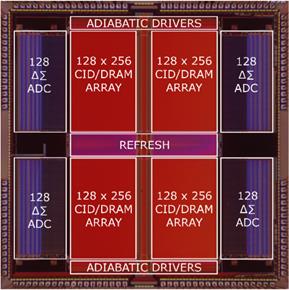
(b)
Figure 6. Examples of our computational back-end
integrated circuits: (a) mixed-signal multi-core DSPs within closed-loop
responsive neurostimulators for treating neurological disorders, and (b)
implantable mixed-signal machine learning accelerators (world’s first support
vector machines in silicon).
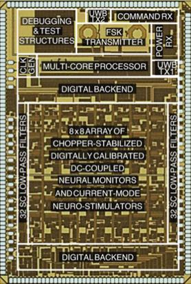
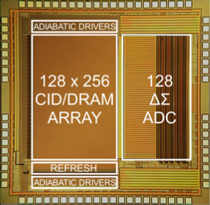
4. Wireless Communication and
Powering Circuits
Sensory microsystems often require wire-free and
battery-free operation under strict constraints of low form factor, high data
rate, high energy efficiency and low specific absorption rate. Our solutions to
these challenges include low-power custom FSK and UWB radio-frequency
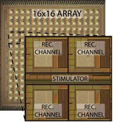
transceivers (Fig. 7a) [J20, J21, J27, C45, C50], as well as wireless energy
transfer circuits for neural recording and neurostimulation with off-chip (Fig
7b) and on-chip (Fig. 7c) RFID-type inductive power/data receiver coils [C55].
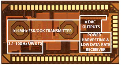
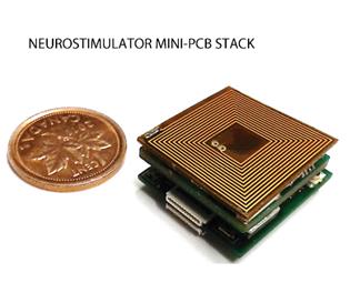
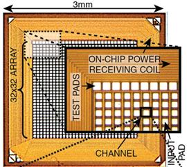
Figure
7. Examples of our RF transceivers and inductive energy transfer microsystems
prototypes: (left) custom radio-frequency transceivers, (middle) inductively
powered wireless neural recording and neurostimulation microsystem, and (right)
inductive power receiving circuits with an on-chip coil.
We
always look forward to having talented graduate students from the University of
Toronto and around the world join our team!
